
NEWS
iPhone 18 Pro Chip Leak Widens Memory for On-Device AI
Solder maps for the iPhone 18 Pro A20 Pro point to seven GPU cores, a frozen six-core CPU, and a 96-bit memory bus aimed at on-device AI.

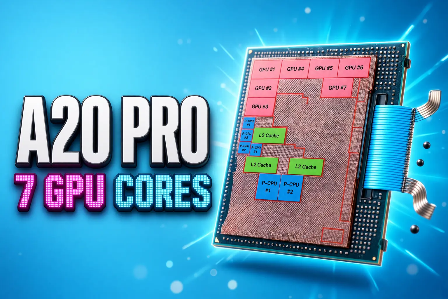
A Weibo reconstruction of iPhone 18 Pro solder maps points to seven GPU cores on the A20 Pro, one more than last year’s chip. The same maps keep a six-core CPU and sketch a much wider path to memory, the part of the design that on-device models actually wait on.
Those maps landed on August 30. Apple’s hardware event is on September 9 at 10 a.m. Pacific Time, so the floorplan is circulating while the company can still confirm, trim, or ignore every block on it.
What the A20 Pro Solder Maps Show
The images are not a photograph of the A20 Pro die. Weibo user Fried White Rice, whose handle is 白饭炒白米饭, overlaid a board’s solder-ball pattern with older Apple die outlines and drew where the CPU, GPU, and memory interface sit. The account has been right on some prior Apple silicon details, and the method is still guesswork: ball grids and outlines, not a lab shot of this chip.
The solder-map reconstruction on Weibo puts LPDDR contacts on the right edge of the package, the GPU along the top of the die, and the CPU in the center. From that outline the account tried more than ten GPU layouts at 6, 7, and 8 cores and picked seven as the fit that wasted the least space.
Ultimately, the 7-core GPU configuration emerges as the most plausible arrangement.
Fried White Rice, Weibo, August 30, 2026
A jump from six GPU cores to seven is about 16% more graphics units, not a new GPU family. The maps do not show clocks, ray-tracing hardware, or whether every iPhone that uses this silicon will enable all seven cores.
WHAT WE KNOW
- The method: The post reconstructs a floorplan from solder-ball positions and older die outlines, not from a new photographed die.
- The CPU count: The outline matches a 2-performance plus 4-efficiency layout, the same six-core split as the A19 Pro.
- The cache call: Efficiency-core L2 is read as 8 MB, up from 6 MB, with performance-core L2 still at 16 MB.
- The bus: The right-edge contacts are read as a 96-bit LPDDR5X interface, up from 64 bits on the A19 Pro.
System-level cache is the hole in the drawing. Fried White Rice said it should not shrink, because the same generation is expected to carry a new image signal processor and a larger Neural Engine, both hungry for shared cache. That is an inference on top of an inference.
WHAT IS UNCONFIRMED
- Final GPU count: Six, seven, and eight cores all fit some of the ball pattern; seven is the leaker’s best guess.
- RAM capacity: Earlier board leaks have held total memory at 12 GB, which these maps do not prove.
- New ISP and Neural Engine: Cited as reasons not to cut system cache, not as measured blocks.
Treat the seven-core figure as a ranked guess. Treat the six-core CPU and the wider memory edge as the parts of the drawing that move the least if a couple of balls are misread.
Apple Still Will Not Add a CPU Core
The A20 Pro, if this outline is right, still has two performance cores and four efficiency cores. That is the same split Apple has used on Pro iPhones since the A17 Pro in 2023, through the A18 Pro in 2024 and the A19 Pro in 2025. The company has been spending transistor budget on graphics, cache, and the Neural Engine while the CPU core count sits still.
The efficiency cores are the ones that get a bigger private stash. Shared L2 for those four small cores is read as 8 MB, 2 MB above the A19 Pro. The two big cores keep 16 MB, drawn as two 8 MB blocks. When background work, dictation, and always-on Apple Intelligence jobs run on the small cores, a fatter L2 means fewer trips out to main memory.
That is a quiet change. It does not show up in a GPU core headline, and it is the kind of tweak that helps sustained on-device work more than a short Geekbench burst. The maps do not say whether the cores themselves are new designs or last year’s cores with more cache beside them.
Apple Widens the Memory Bus to 96 Bits
The right edge of the package is the loud part of the drawing. The A19 Pro talks to LPDDR5X over a 64-bit interface. The A20 Pro maps point to a 96-bit interface on LPDDR5X, which is 50% more width if the memory clocks stay in the same band.
Apple is not taking the LPDDR6 step in this reading. A June motherboard leak had put LPDDR6 on a 96-bit bus; the August solder maps, which are newer, keep LPDDR5X and still draw the wider bus. Bandwidth then comes from width, and maybe from a faster LPDDR5X grade, not from a new memory standard.
THE BUS IN PLAIN NUMBERS
- A19 Pro interface: 64-bit LPDDR5X, the width Apple has used on recent Pro chips.
- A20 Pro reading: 96-bit LPDDR5X, a 50% wider path on the same memory family.
- What that feeds: GPU tiles, the Neural Engine, and local language models that stall when the bus is narrow.
- What it does not settle: Clock speed, total gigabytes, or whether every SKU gets the full bus.
On-device models are memory-bound long before they are core-bound. A seventh GPU core helps if the bus can keep it busy; a 50% wider bus helps even if the GPU count had stayed at six. Reconstructing a floorplan from solder balls is a coarse tool, and the memory edge is the coarsest, most physical part of that tool, which is why the 96-bit call is sturdier than the GPU core census.
Efficiency-Core Cache Has Grown Since the A17 Pro
Put the A20 Pro guess next to the last three Pro chips and the pattern is blunt. CPU cores do not move. GPU cores barely move. The small-core cache keeps stepping up, and this year the GPU finally gains a core while the memory bus jumps a third of a width.
PRO IPHONE SILICON, A17 TO A20
| Chip | CPU | GPU cores | E-core L2 | P-core L2 | Memory bus |
|---|---|---|---|---|---|
| A17 Pro (2023) | 2P + 4E | 6 | 4 MB | 16 MB | 64-bit class |
| A18 Pro (2024) | 2P + 4E | 6 | 4 MB | 16 MB | 64-bit class |
| A19 Pro (2025) | 2P + 4E | 6 (5 on iPhone Air) | 6 MB | 16 MB | 64-bit |
| A20 Pro (maps, 2026) | 2P + 4E | 7 | 8 MB | 16 MB | 96-bit LPDDR5X |
The Air already showed how Apple bins this GPU. The iPhone Air uses A19 Pro silicon with one graphics core off, a 5-core GPU against six on the 17 Pro. A seven-core A20 Pro gives the company the same trick on the next thin phone: ship seven on the 18 Pro and 18 Pro Max, fuse one off where the chassis cannot cool it.
E-core L2 is the other ladder. It held at 4 MB on the A17 Pro and A18 Pro, rose to 6 MB on the A19 Pro, and is drawn at 8 MB here. That is a doubling across three years on the cores that own background and always-on work, which is where Apple Intelligence actually lives between user taps.
The 18% Speed Claim Mixes Two TSMC Figures
A separate Weibo account, Fixed Focus Digital, said on August 17 that supply-chain sources put the A20 Pro about 18% faster than the A19 Pro and about 30% better on power. Those two numbers have been repeated as if they arrive together. TSMC’s own node copy does not sell them that way.
The A20 Pro is expected to be Apple’s first iPhone chip on TSMC’s 2-nanometer N2 family, with gate-all-around nanosheet transistors. TSMC’s N2 paper describes a full-node step from 3-nanometer as a 15% speed gain or a 30% power cut, with more than 1.15 times chip density. The word in the middle is or. A designer can spend the node on clocks, on watts, or on some of each, and less of both.
N2 delivers a full node benefit from previous 3nm node in offering 15% speed gain or 30% power reduction with >1.15x chip density increase.
TSMC N2 platform paper, research.tsmc.com
The 18% figure sits closer to a different TSMC line. On its HPC platform page, TSMC says N2P, a faster N2 variant, delivers an 18% speed improvement at the same power against N3E, plus a larger power cut if clocks hold still. The A19 Pro is an N3P chip, not an N3E chip, so even that 18% is a node-marketing number, not a measured A20 Pro versus A19 Pro result.
Apple usually splits CPU, GPU, and Neural Engine gains on stage. Until it does, the honest read of Fixed Focus Digital is that someone in the chain copied TSMC’s node slide and applied it to a product. The solder maps do not prove 18% or 30%. They only show where Apple spent area: one GPU core, more small-core cache, and a fatter memory edge.
Side-by-Side Memory Leaves Finished Silicon Waiting
The wider bus is not a free overlay on last year’s package. Apple is moving the A20 Pro from the old fan-out stack, where DRAM sat on top of the SoC, to wafer-level multi-chip modules, or WMCM. Memory dies sit beside the processor in the same package, which eases the heat that used to cook both chips in a vertical sandwich and lets the bus grow to 96 bits without stacking more height.
Chip watcher Reptalica posted board photos of that layout on June 26, with DRAM shifted off the processor and a 96-bit memory path already drawn.
https://x.com/Reptalicant/status/2070494675258274257
WHAT WMCM CHANGES ON THIS CHIP
- Placement: DRAM moves beside the SoC instead of sitting on top of it.
- Heat: The processor and memory no longer dump into the same vertical stack during long GPU or model runs.
- Bus width: A 96-bit interface needs more package edge, which the side-by-side layout can give it.
- The bind: The chip and its DRAM have to meet at the wafer stage, so missing memory stops the package, not just the phone line.
That last point is the cost of the architecture. Taipei journalist Tim Culpan wrote in early August that N2 output for the A20 Pro was healthy, then stalled in packaging because LPDDR5X was late, leaving about $1 billion of A20 Pro silicon waiting on DRAM. TSMC CFO Wendell Huang had told investors on the July 16 earnings call that inventory days rose seven to 87, “primarily due to the ramp of N2 technology.”
Analyst Ming-Chi Kuo pushed back on a giant idle pile, arguing Apple and TSMC size wafer starts to the DRAM they can get. He still put A20 series pull-in about 10% to 20% under the original plan from the second half of 2026 into early 2027, because LPDDR is tight. Apple buys that memory from Micron, SK Hynix, and Samsung, the same pool AI server builds have been draining.
The iPhone 18 Pro’s wider, faster LPDDR5X package is a bigger memory buy after the memory squeeze on last year’s iPhones already tested how far Apple would push price to cover DRAM. The maps make that bill larger. They also make the phone more dependent on a part TSMC cannot print in the N2 bay.
The Foldable May Ship With One GPU Core Off
The A20 Pro is expected in the iPhone 18 Pro, the iPhone 18 Pro Max, and Apple’s first foldable, widely called the iPhone Ultra. A seven-core GPU is a gift to the two slab phones and a problem for a hinge-thin body. The Air already proved the bin: same silicon, one GPU core disabled where thermals run out.
If the maps are right, the Ultra is the obvious candidate for a 6-core cut of this chip. The extra core is then a Pro-and-Max feature, not a family-wide one, which makes the “seven-core GPU” headline true for some phones and false for the thinnest one on the same stage.
Apple has already put the date on a card. Greg Joswiak posted the Surprise and Shine event on September 9, 10 a.m. Pacific, from Apple Park. That is where the company will either read out GPU cores, memory bandwidth, and 2-nanometer efficiency in its own units, or skip the floorplan and talk about cameras and a foldable instead.
Until then the solder maps are a ranked guess with one solid physical tell. Apple is still unwilling to add a CPU core, and it is spending package edge, cache, and DRAM supply on the path that feeds graphics and local models. The seventh GPU core is what fits in the remaining outline.


Companies Froze Job Design and Called AI a People Problem

Xiaomi’s Own Chip Lands While Apple Argues Over Color

Pixel 11 Trails Galaxy Phones That Last as Long

Tecno Camon Slim 5G Repeats Artist Colors on New 5G Hardware

Bushel Finds Farm AI Living in the Office

AI Made Feature Moats Cheap and Left Trust Standing

OpenAI’s Research Intern Arrives With a Warning Attached

Robinhood Prices XRP Into a Two-Cent 9 a.m. Bet

Japan’s First Atom Quantum Computer Runs on Infleqtion’s QPU

Pride and Soul Follows Konami’s Locked 2026 Core Formula

Oracle Cuts 21,000 Jobs in a Year, Cites AI in 10-K Filing

Fable 5 and Mythos 5 Return as US Lifts Anthropic Export Controls

SpaceX’s Google Deal Turns a Rocket Company Into a Cloud Landlord

CD Projekt Red Co-CEO: Redemption Arc Isn’t Done, Witcher 4 in 2027

XPL Rallies 30% Ahead of Plasma One Card Tier Launch

Google Search Profiles Build a Follow Graph Inside Discover

DGO App Brings Rs 549 Mobile Pass for FIFA World Cup 2026 in Nepal

Moonshot AI Targets $30 Billion in China’s Fastest AI Funding Sprint

Oppo’s ColorOS 17 Eligibility List Leaves A-Series Buyers Behind

Microsoft Xbox Layoffs Start in July as Sharma Slams 3% Margin
-
 AI3 months ago
Oracle Cuts 21,000 Jobs in a Year, Cites AI in 10-K Filing
-
 AI2 months ago
Fable 5 and Mythos 5 Return as US Lifts Anthropic Export Controls
-
 AI3 months ago
SpaceX’s Google Deal Turns a Rocket Company Into a Cloud Landlord
-
 GAMING3 months ago
CD Projekt Red Co-CEO: Redemption Arc Isn’t Done, Witcher 4 in 2027
-
 CRYPTO3 months ago
XPL Rallies 30% Ahead of Plasma One Card Tier Launch
-
 NEWS3 months ago
Google Search Profiles Build a Follow Graph Inside Discover
-
 APPS3 months ago
DGO App Brings Rs 549 Mobile Pass for FIFA World Cup 2026 in Nepal
-
 AI3 months ago
Moonshot AI Targets $30 Billion in China’s Fastest AI Funding Sprint