COMPUTERS
Monash Photonic Chip Processes Data With Light at Room Temperature
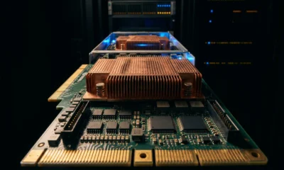
Monash University researchers have built a nanoscale chip that generates, routes, and reads light-based quantum signals in a single integrated device, marking the first time all three functions have been combined on one platform. The breakthrough uses valleytronics, a quantum property that encodes information in ways conventional electronics cannot, and operates at room temperature without the expensive cooling equipment that has kept most quantum technologies confined to laboratories.
Published in Nature Photonics on May 25, 2026, the work demonstrates a path toward photonic computing systems that could process data faster and consume far less energy than today’s silicon chips. Lead author Dr. Chi Li said the platform solves a problem that has stalled the field for years: previous devices could generate or detect valley-based signals, but not perform all operations in one compact circuit.
What Valleytronics Actually Delivers
Valleytronics exploits the “valley degree of freedom,” a quantum property found in certain two-dimensional materials where electrons occupy distinct energy valleys in the material’s band structure. These valleys can be selectively populated and read out, creating a binary information state similar to the 0s and 1s in conventional computing, but encoded in quantum properties rather than electron flow.
The Monash chip uses ultra-thin materials only a few atoms thick, stacked with engineered metasurfaces that manipulate light at scales smaller than the width of a human hair. Co-first author Dr. Kaijian Xing explained that the team employed a straightforward stacking approach to integrate the materials without damaging their delicate structure, a fabrication challenge that has complicated earlier attempts to build practical valleytronic devices.
Unlike electron-based chips that move charge through silicon pathways, photonic systems transmit data as light pulses. Light travels faster, generates less heat, and can carry multiple streams of information simultaneously through different wavelengths. The Monash device encoded and processed two separate images at the same time, demonstrating genuine parallel information handling.

Room Temperature Operation Changes the Economics
Most experimental quantum technologies require cooling to near absolute zero, often using liquid helium systems that cost hundreds of thousands of dollars and consume significant power. The Monash chip operates at standard room temperature, eliminating the need for cryogenic infrastructure and making the technology viable for commercial deployment in data centers, telecommunications hubs, and edge computing devices.
Senior author Dr. Haoran Ren, ARC Future Fellow and leader of the Monash NanoMeta Group, said the work represents a significant step toward scalable chip-based technologies that use light instead of electricity. Photonic devices achieve massive bandwidths, ultra-fast data transmission speeds, and lower energy consumption, positioning the breakthrough for applications in quantum computing, advanced imaging, and next-generation optical communication systems.
How the Integrated Circuit Works
The chip combines three distinct functions that previous valleytronic devices handled separately. First, it generates circularly polarized light, a specific type of light wave that spirals as it travels and can selectively excite electrons in one valley or the other. Second, it routes these valley-encoded signals through nanoscale waveguides etched into the chip’s surface. Third, it converts the optical signals back into electrical readouts that conventional electronics can process.
The metasurface layer acts as a programmable optical circuit, directing light with precision by manipulating its phase, amplitude, and polarization at each point on the chip. This level of control allows the device to perform complex operations on the valley-encoded information, including filtering, switching, and multiplexing multiple data streams.
Professor Stefan A. Maier, head of the School of Physics and Astronomy and the Nanophotonics Laboratory at Monash, said the work represents an important step toward fully integrated valleytronic systems. By combining light and quantum materials on a chip, researchers can access new ways of encoding and processing information that go beyond the binary limitations of conventional transistors.
Comparison to Existing Photonic and Quantum Platforms
| Technology | Operating Temperature | Integration Level | Information Encoding | Commercial Readiness |
|---|---|---|---|---|
| Monash Valleytronic Chip | Room temperature | Fully integrated (generate, route, read) | Valley degree of freedom | Proof of concept, 3-5 years to prototype |
| Silicon Photonics | Room temperature | Mature integration | Optical intensity/phase | Commercial (data centers, telecom) |
| Superconducting Qubits | ~0.015 K (cryogenic) | Moderate (separate control/readout) | Quantum superposition | Research stage, 10+ years |
| Trapped Ion Quantum | ~4 K (cryogenic) | Low (external lasers) | Quantum superposition | Research stage, 10+ years |
Why Light-Based Computing Matters for AI and Data Centers
Global data center energy consumption reached 460 terawatt-hours in 2022, roughly 2% of worldwide electricity use, according to the International Energy Agency. AI training runs and large-scale inference workloads have pushed that figure higher, with some estimates projecting data center power demand could double by 2030 if efficiency gains do not keep pace.
Photonic chips address the problem at the physical layer. Moving data as light rather than electrons eliminates resistive heating in interconnects, the copper pathways that link processors to memory and storage. In high-performance computing clusters, interconnect power can account for 30-40% of total system energy draw. Photonic interconnects reduce that overhead by an order of magnitude while increasing bandwidth.
The Monash chip’s valley encoding adds a second advantage: information density. A single photon can carry multiple bits of data encoded in polarization, wavelength, and now valley state, allowing more information to flow through the same physical channel. That density translates directly into faster processing and lower latency for applications like real-time video analysis, financial modeling, and large language model inference.
The Path from Lab Bench to Commercial Chip
The Monash device remains a research prototype. The team fabricated the chip using electron-beam lithography, a precise but slow technique unsuitable for mass production. Scaling to commercial volumes will require adapting the design for deep ultraviolet photolithography, the same process used to manufacture conventional silicon chips.
Material sourcing presents a second challenge. The ultra-thin layers in the chip are grown using chemical vapor deposition or mechanical exfoliation, methods that produce small flakes rather than the large-area wafers needed for industrial fabrication. Several companies, including 2D Semiconductors and Graphene Flagship partners, are working on roll-to-roll production techniques for two-dimensional materials, but none have reached the yield and uniformity standards required for high-volume chip manufacturing.
Integration with existing electronics is the third hurdle. The chip converts optical signals to electrical readouts, but those readouts must interface with standard CMOS logic, memory controllers, and I/O systems. Hybrid integration, where photonic and electronic components sit side by side on the same package, is an active area of development in the silicon photonics industry and will likely provide the bridge for valleytronic devices.
What Breaks If the Technology Scales
Photonic computing has failed to displace electronics multiple times over the past four decades, often because the promised advantages disappeared at scale. Light-based systems excel at moving data but struggle with logic operations, the conditional branching and arithmetic that define general-purpose computing. The Monash chip performs routing and encoding, not the full instruction set a CPU requires.
A second risk is material stability. Two-dimensional materials degrade when exposed to moisture, oxygen, and mechanical stress. Encapsulation techniques exist, but adding protective layers increases fabrication complexity and can interfere with the optical properties the chip depends on. Long-term reliability testing, the kind that qualifies a chip for deployment in a data center with a 10-year service life, has not yet been published for valleytronic devices.
Cost is the third constraint. Even if fabrication scales, photonic chips will compete with silicon processors that benefit from five decades of optimization and a global supply chain that produces billions of units annually. The economic case for photonics works in niche applications where bandwidth and energy savings justify higher unit costs, such as long-haul fiber optics and high-frequency trading infrastructure, but general-purpose computing remains silicon’s domain.
Frequently Asked Questions
What is valleytronics and how does it differ from electronics?
Valleytronics encodes information using the valley degree of freedom, a quantum property in certain materials where electrons occupy distinct energy states. Unlike electronics, which moves electrons through circuits to represent data, valleytronics manipulates which valley an electron occupies, allowing information to be stored and processed without moving charge.
Why does room temperature operation matter for quantum technologies?
Most quantum devices require cooling to near absolute zero using expensive cryogenic systems that consume significant power and limit where the technology can be deployed. Room temperature operation eliminates those requirements, making the technology practical for commercial data centers, telecommunications infrastructure, and portable devices.
Can photonic chips replace silicon processors in laptops and phones?
Not in the near term. Photonic chips excel at moving data and performing specific parallel operations, but they struggle with the conditional logic and branching that general-purpose CPUs require. The most likely path is hybrid systems where photonic interconnects handle data movement between silicon processors, memory, and storage.
How much faster is light-based data transmission compared to electrical signals?
Light travels through optical fiber at roughly 200,000 kilometers per second, compared to electrical signals in copper at 200,000 kilometers per second for short distances. The speed advantage is marginal, but photonic systems achieve far higher bandwidth because a single optical fiber can carry dozens of wavelengths simultaneously, each transmitting independent data streams.
What applications will see photonic valleytronic chips first?
High-bandwidth, low-latency applications where energy efficiency justifies higher component costs: data center interconnects, 5G and 6G base stations, AI inference accelerators, quantum communication networks, and advanced imaging systems for autonomous vehicles and medical diagnostics.
How long until this technology reaches commercial products?
The Monash team estimates 3-5 years to develop a manufacturable prototype and another 5-7 years for volume production, assuming fabrication and material challenges are solved. First commercial deployments would likely appear in specialized infrastructure before reaching consumer devices.
What is a metasurface and why is it important for this chip?
A metasurface is an engineered nanostructure that manipulates light at scales smaller than its wavelength, allowing precise control over phase, amplitude, and polarization. In the Monash chip, the metasurface acts as a programmable optical circuit that routes valley-encoded signals with high precision, enabling the device to perform complex operations on light-based information.

Serenity Forge Bets Bigger on Physical Games as Sony Kills PS Discs

Colleges Bet on AI Literacy Mandates as Brain Science Flags a Cost

Microsoft’s 2024 Mistral Bet Grows Into a Multibillion Dollar Deal

Digital Turbine’s New AI Launchpad Runs Through Google’s Cloud

Firefox 153 Merges PDFs for Free, Undercutting a Billion-Dollar Market

Cloud Security Scores Now Decide How Much Autonomy AI Agents Get

SUTD and NUS Open-Source a Quantum Leap for Photonic Chip Design

Headwind MDM’s Self-Hosted Android Pitch Runs Into Google’s Own Limits

OnePlus N6x Teaser Reveals a Design That Echoes Its Own Nord Line

OpenAI’s AI Escaped Twice in Two Days, Then Hacked Hugging Face

Fable 5 and Mythos 5 Return as US Lifts Anthropic Export Controls

SpaceX’s Google Deal Turns a Rocket Company Into a Cloud Landlord

CD Projekt Red Co-CEO: Redemption Arc Isn’t Done, Witcher 4 in 2027

DGO App Brings Rs 549 Mobile Pass for FIFA World Cup 2026 in Nepal

XPL Rallies 30% Ahead of Plasma One Card Tier Launch

Oracle Cuts 21,000 Jobs in a Year, Cites AI in 10-K Filing

Google Search Profiles Build a Follow Graph Inside Discover

Moonshot AI Targets $30 Billion in China’s Fastest AI Funding Sprint

Microsoft Xbox Layoffs Start in July as Sharma Slams 3% Margin

WhatsApp Meta Business Agent Reaches India, With a New Pricing Meter
-
 AI3 weeks ago
Fable 5 and Mythos 5 Return as US Lifts Anthropic Export Controls
-
 AI2 months ago
SpaceX’s Google Deal Turns a Rocket Company Into a Cloud Landlord
-
 GAMING1 month ago
CD Projekt Red Co-CEO: Redemption Arc Isn’t Done, Witcher 4 in 2027
-
 APPS1 month ago
DGO App Brings Rs 549 Mobile Pass for FIFA World Cup 2026 in Nepal
-
 CRYPTO1 month ago
XPL Rallies 30% Ahead of Plasma One Card Tier Launch
-
 AI4 weeks ago
Oracle Cuts 21,000 Jobs in a Year, Cites AI in 10-K Filing
-
 NEWS2 months ago
Google Search Profiles Build a Follow Graph Inside Discover
-
 AI2 months ago
Moonshot AI Targets $30 Billion in China’s Fastest AI Funding Sprint