COMPUTERS
Platinum-Copper Stack Vibrates at One Terahertz Under a Laser
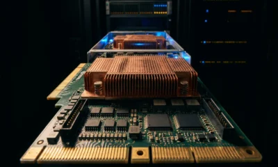
A laser pulse set platinum-copper layers vibrating at one terahertz with 1% strain, and electron pressure, not heat, was the driver. The films were sputtered.
A laser pulse can shake a stack of platinum and copper layers into vibrating roughly a trillion times a second. Researchers at European XFEL and the University of Potsdam reported on June 18, 2026, that they set a layered metal sample oscillating at around one terahertz, with the platinum layers expanding and the copper layers compressing on each cycle. The atoms displaced by 1% on average from their resting positions, a strain amplitude the paper calls giant.
The result, published in Nature Communications, points to a new route to manipulating materials for next-generation computing, and it works by a mechanism the team did not expect. Electron pressure, not heat, drove the terahertz motion, and the platinum-copper films were made by sputtering, the same industrial process already used to coat microchips and glass. The combination, an electronically driven mode and a fab-friendly fabrication, suggests the gap between a lab demonstration and a manufactured device may be shorter than usual for a physics result.
A One-Trillion-Times-a-Second Oscillation
The headline result is a coherent lattice vibration at roughly one terahertz, a regime where most metals cannot support a clean structural wave. The team stacked 2.5 nanometres of platinum and 2.3 nanometres of copper into an artificial lattice, then hit it with a femtosecond laser pulse at 800 nanometres wavelength. The optical energy was absorbed mainly in the platinum layers, and the entire stack responded as a single coherent mode.
The amplitude of the oscillation reached 1% of the lattice spacing, a number the paper describes as “giant” for an ultrafast strain measurement. The frequency, just under one terahertz, was set by the layer thicknesses and the sound velocities of the two metals, and matched the prediction of a simple wave equation based on those numbers. That agreement matters because it tells the reader the vibration is a structural mode of the superlattice as a whole, not a property of one metal alone. The mode wavelength sits below the optical skin depth of both metals, which keeps the wave narrow-band and coherent, since a broadband pulse would otherwise radiate away from the surface.
The full data set and modelling appear in the published study of the platinum-copper superlattice in Nature Communications on June 18, 2026. The superlattice sat on a thicker copper layer and a thin nickel capping layer, both used as built-in diagnostics. The nickel tracks where the deposited energy ends up, and the data show the energy does travel through the copper into the nickel, just not before the terahertz wave gets going. The frequency was a prediction before it was a measurement, derived from the layer thicknesses and the metals’ sound velocities. The measured frequency came in just under 1 THz, matching the prediction.

The Surprise in the Data
The team did not set out to find electron pressure as the driver. Conventional models treat a metal under laser excitation as a hot lattice warmed by electron-phonon coupling, in which case the strain wave should begin with a measurable delay as heat diffuses from the electrons into the atoms. The platinum-copper data did not fit that picture.
The diffraction measurements showed the oscillation starting with nearly zero phase shift after the laser pulse, the signature of a quasi-instantaneous stress applied before any significant heat transfer has had time to occur. That delay-free start is what terahertz-frequency strain engineering needs to be useful, because slower heat-driven mechanisms wash out the higher harmonics and limit how fast a structure can be modulated. The same finding reframes the practical question, putting the focus on the position and energy of the electrons inside the metal. The team had been expecting the standard picture, in which heat from the electrons diffuses into the lattice over a picosecond.
That surprised us. The oscillation is not caused by the pressure of the heated lattice, but by electron pressure, particularly in the platinum layers.
The quote is from Jan-Etienne Pudell of European XFEL, the study’s first author, in the institute’s write-up of the platinum-copper result. A marginal correction would not have explained a 1% strain wave with near-zero phase delay. The platinum-copper stack did not heat up before it expanded, and the strain wave began on the timescale of electron-electron thermalisation. The finding reframes the practical question for high-frequency strain engineering, putting the focus on where the excited electrons sit and how much momentum they can deliver. The Bargheer group at the University of Potsdam weighed in with a plainer physical description of the same observation.
We’re not simply seeing a metal heating up and expanding here. We see that the electrons themselves exert pressure within less than one trillionth of a second, and in a way pound from within on the surface of the metal. This is highly exciting for the chemistry of nanometres thin metal layers, because it sheds new light on the question of hot electrons, heat, atomic movements all the way to chemical reactions.
The quote is from Matias Bargheer, spokesperson for the Collaborative Research Centre (SFB) 1636 “Elementary Processes of Light-Driven Reactions at Nanoscale Metals” at the University of Potsdam. The Bargheer group built the modelling side of the paper, with the density-functional theory calculations that confirm electron-phonon coupling is too slow to drive the observed oscillation on its own. The X-ray data and the DFT calculation are independent lines of evidence for the same mechanism.
The electron-pressure picture rests on three legs: the near-zero phase delay in the diffraction data, the speed-of-sound mismatch between heat and lattice motion, and the DFT prediction of slow electron-phonon coupling. The wave begins before any of that heat can reach the lattice, which lets the strain amplitude reach 1%. The result extends to a fully metallic system a finding first made in semiconductors, where photoexcited carriers were shown to propagate as stress gradients. Metals, under the right conditions, can be kicked by their own electrons, and the new study shows it at 1 THz.
Why Platinum and Copper
The choice of platinum and copper was not arbitrary. Platinum holds a large amount of electronic energy when excited, and copper lets electrons move through it with very little resistance. Stacking the two in nanometre-thick layers puts those two properties side by side, so the energy deposited by the laser can be focused into the platinum while the copper stays relatively cool and compliant. The combination also gives the wave something to push against, since copper’s compliance lets the platinum expansion compress the copper layer on each cycle. The paper’s authors call the structure a thermoacoustic metamaterial, a synthetic solid whose acoustic and thermal behaviour is tuned at the atomic scale.
The geometry does most of the rest. The optical skin depth in these metals is on the order of ten nanometres, and the superlattice period is below five. That sub-skin-depth structure is what allows a narrow-band coherent mode to build up, with a broadband strain pulse radiating away from the surface under different conditions. The frequency, around one terahertz, is set by the layer thicknesses and the sound velocities of the two metals, which is why changing the deposition recipe can re-target the wave to a different frequency.
The X-ray Proof at MID
The experiment ran at the Materials Imaging and Dynamics (MID) instrument at European XFEL, an X-ray free-electron laser facility in Schenefeld, Germany. MID produces ultrashort hard X-ray pulses in synchrony with the optical pump laser, so the team could take an X-ray snapshot of the lattice at controlled delays after each laser pulse. The X-rays penetrate the whole stack and scatter off specific atomic planes, giving a depth-resolved signal that no optical probe can match in a metal.
The key measurement was the position and intensity of the superlattice’s Bragg peaks, the X-ray reflections that come from the periodic platinum-copper structure. The (0 0 23) superlattice peak dropped by 15% within about half a picosecond, the direct fingerprint of the platinum layers expanding to 1% of the lattice spacing. The first half-period of the 1 THz oscillation showed up in the very first time step, with nearly zero phase, exactly the pattern expected from a quasi-instantaneous electron-pressure kick. A delayed thermal expansion would arrive with measurable delay. The (0 0 22) peak oscillated at the same frequency and phase but in the opposite direction, an independent confirmation that the entire superlattice was moving as a single mode.
“The MID instrument was built precisely to address questions such as: How do atoms and electrons move in complex materials when they are brought out of equilibrium by light?” Pudell says. The platinum-copper run is one of the cleaner demonstrations of that capability so far, because the geometry of the sample let the team separate the platinum response from the copper response in a single diffraction pattern, and most ultrafast strain measurements in metals average over the optical penetration depth. The technique is now being applied to a wider class of layered metals, with the platinum-copper result as the proof that the approach can isolate a single coherent THz mode.
The X-ray data also rule out a phonon-driven picture for the wave. A phonon-driven oscillation would arrive with a measurable delay, set by the time it takes heat to diffuse from the electrons into the lattice. The data show no such delay. The team therefore identifies electron pressure as the dominant driver.
The Sputtering Shortcut
The superlattice was sputtered, the same physical vapour deposition process fabricators use to put down barrier layers, reflective coatings, and interconnects on everything from flat-panel displays to magnetic hard drives. The paper describes all-metallic superlattices as “straightforward to fabricate by sputtering,” which is a careful way of saying that anyone with a deposition chamber can make one. The deposition route matters because most strain-engineering breakthroughs sit on the wrong side of the manufacturing divide, where the physics works in a vacuum chamber held together by hand-built samples but the materials system does not survive contact with a real fab. The platinum-copper stack does, in principle, survive that contact, and the same toolset that already coats chips and glass can in principle make a run of them. The technique can tune the layer thicknesses to land on a different frequency, the paper notes, and the metals themselves are not exotic.
The paper positions the new study inside the broader field of thermoacoustic metamaterials, nanostructured solids designed to manipulate sound and heat in ways ordinary solids cannot. So far the field has mostly been explored at lower frequencies, where thermal expansion is fast enough to drive the response. The new work adds a high-frequency, electronically driven mode to that class of materials, at room temperature, in a fully metallic system.
There is a second reason sputtering matters here, and it has to do with the metals themselves. Platinum and copper are both well-understood sputtering targets with established purity and uniformity standards. Sputtering also makes it straightforward to cap the superlattice with a different metal, such as the thin nickel layer the team used as a built-in thermometer. The same flexibility is what makes giant magnetoresistance stacks, spin valves, and THz spintronic emitters practical at industrial scale today.
What THz Strain Buys Spintronics
The application the paper names is spintronics, the family of devices that store and move information using the magnetic spin of electrons rather than their charge. Spintronic devices already work, including the giant magnetoresistance read heads that lifted hard-drive density two decades ago and the THz spintronic emitters now in research labs. A controllable strain wave at 1 THz could, in principle, shake spins into alignment or out of alignment faster than magnetic fields can. The paper does not claim to have built such a device, and the work is best read as establishing a precondition for one. The remaining test is whether the same mechanism survives in a working device structure, ideally one that can be deposited directly on a chip-relevant substrate.
The paper’s authors write that the same logic could address “quasiparticles in the THz range via strain to effectuate, e.g., superconductivity or spin dynamics,” and could be added to synthetic ferrimagnets as the layer period approaches a few atomic layers. The applications named in the paper sit inside the envelope of materials the sputtering process already supports. The list runs four families long, and each one is an active research area in its own right.
- Spintronic emitters, which already use metal-metal interfaces to generate THz radiation in research labs
- Synthetic ferrimagnets, where strain could complement magnetic switching as layer periods approach a few atomic layers
- Plasmonic chemistry, where hot-electron pressure is a candidate pathway for moving energy into molecules sitting on the platinum surface
- THz-frequency acoustics of layered metals, a broader class the platinum-copper result opens up
Bargheer frames the chemistry implication as the second piece of the story. “This creates a new experimental and conceptual link between plasmonic chemistry, the dynamics of high-energy electrons, heat flow and ultrafast structural changes,” he says. The hot-electron pressure at the platinum surfaces, the mechanism behind the terahertz wave, is also a candidate pathway for moving energy into molecules sitting on those surfaces. The same physics that drives the strain could drive a chemical reaction, so the same metal layer can be studied as both an acoustic metamaterial and a plasmonic substrate.
The paper’s framing is deliberately narrow. It claims that strain waves at terahertz frequencies can be made coherent, large amplitude, and electronically addressable in a fully metallic superlattice. It stops short of claiming they have been used in a spintronic device. Whether that precondition turns into a real spintronic or superconducting device will depend on follow-up work, and the paper itself does not commit to a timeline for any of it.
What’s Still Open
The result is a proof of mechanism, with a packaged device still ahead. The strain wave runs at room temperature but only in a sample small enough to fit in a beamline chamber, and only for the few picoseconds before heat transport damps it out. Scaling up means answering at least three open questions: how long the coherence holds in a thicker film, how the efficiency changes at repetition rates higher than the few kilohertz MID can run, and whether the same electron-pressure mechanism survives when the superlattice is buried under real device layers rather than sitting at the surface of a custom sample. The deeper challenge is the one the paper itself acknowledges: electron pressure has now been shown to dominate at one specific frequency and one specific pair of metals.
Whether the same trick generalises to other terahertz frequencies, other material combinations, or other applications is the work that has to follow. The paper’s density-functional theory calculations give a starting point for that search, by predicting which metals will hold enough electronic energy to act as the pressure source. The platinum-copper result is now a measurement, and the next round of work will test how general the mechanism is.
Frequently Asked Questions
What is terahertz strain engineering?
In the new platinum-copper study, the lattice oscillates at roughly one terahertz, or about one trillion cycles per second. Terahertz strain engineering is the practice of mechanically distorting a material’s atomic lattice trillions of times per second, fast enough to be useful for next-generation electronics and spintronics. The label refers to a frequency regime where most conventional heating-based approaches fail, because the metal’s free electrons spread the energy too quickly.
What is a metal-metal superlattice?
The new study uses 2.5 nanometres of platinum and 2.3 nanometres of copper, repeating many times to form a stack. A metal-metal superlattice is a synthetic material built from alternating nanometre-thick layers of two different metals. The same kind of layered construction is already used in spintronic read heads and magnetic sensors.
Why is electron pressure surprising?
In the platinum-copper stack, the oscillation started with almost no phase delay, which means the electrons themselves were exerting a quasi-instantaneous force on the atoms rather than just heating them. In most metals, energy from a laser pulse spreads through the free electrons before it has time to push on the lattice, so the structural response looks like thermal expansion with a measurable delay. The new finding shows that metals, under the right conditions, can be kicked by their electrons faster than heat can heat them.
Could this be used in next-generation computers?
The paper does not claim a working device. It claims that coherent, large-amplitude, electronically driven THz strain waves can be made in a fully metallic film, which is a precondition for using strain to control spins or other THz-frequency quasiparticles. Whether that precondition turns into a real spintronic or superconducting device will depend on follow-up work that the paper itself does not commit to a timeline for.
When might this reach devices?
The paper gives no timeline. The Materials Imaging and Dynamics instrument at European XFEL is a one-of-a-kind user facility, and the experiments ran at single-shot or low-repetition rates. Scaling to a process that could land a working device in a fab will likely take years of follow-on work in faster sources, in longer-lived strain waves, and in materials systems beyond platinum and copper.

NotebookLM Becomes Gemini Notebook, and Its New Power Has a Catch

Epic Games Store’s Mobile Freebies Mask a Bigger App Store War

OnePlus Keeps Supporting Existing Owners as Its US Forum Closes

Apple’s Siri AI Reaches the Public, Two Years and $250 Million Later

Honor Bets Its AI Comeback on a Robot Phone That Nods and Dances

Blue Angels Pilot Faces No Discipline After Low Pensacola Beach Pass

OpenAI’s $230 Codex Micro Keypad Signals a Bigger AI Hardware Trend

Apple’s First OLED iPad Mini Arrives by October With a 60Hz Catch

Newgen Software Targets 23-25% Margins as Profit Beats, Stock Slips

HYPE Drops 9% and Robinhood’s CASHCAT Meme Coin Crashes 52%

SpaceX’s Google Deal Turns a Rocket Company Into a Cloud Landlord

XPL Rallies 30% Ahead of Plasma One Card Tier Launch

Google Search Profiles Build a Follow Graph Inside Discover

Microsoft Xbox Layoffs Start in July as Sharma Slams 3% Margin

Oracle Cuts 21,000 Jobs in a Year, Cites AI in 10-K Filing

Moonshot AI Targets $30 Billion in China’s Fastest AI Funding Sprint

WhatsApp Meta Business Agent Reaches India, With a New Pricing Meter

Oppo’s ColorOS 17 Eligibility List Leaves A-Series Buyers Behind

Google DeepMind and A24 Sign $75 Million AI Partnership Deal

Meta’s Iris AI Chip Enters Production in September, Tests Clean
-
 AI1 month ago
SpaceX’s Google Deal Turns a Rocket Company Into a Cloud Landlord
-
 CRYPTO1 month ago
XPL Rallies 30% Ahead of Plasma One Card Tier Launch
-
 NEWS1 month ago
Google Search Profiles Build a Follow Graph Inside Discover
-
 GAMING1 month ago
Microsoft Xbox Layoffs Start in July as Sharma Slams 3% Margin
-
 AI3 weeks ago
Oracle Cuts 21,000 Jobs in a Year, Cites AI in 10-K Filing
-
 AI1 month ago
Moonshot AI Targets $30 Billion in China’s Fastest AI Funding Sprint
-
 AI1 week ago
WhatsApp Meta Business Agent Reaches India, With a New Pricing Meter
-
 NEWS1 month ago
Oppo’s ColorOS 17 Eligibility List Leaves A-Series Buyers Behind