
COMPUTERS
IBM Unveils World’s First Sub-1nm Chip Built on a 3D Nanostack
IBM says its 0.7nm nanostack chip packs nearly 100 billion transistors and runs 70% more efficiently than its 2nm chip, but production is years away.

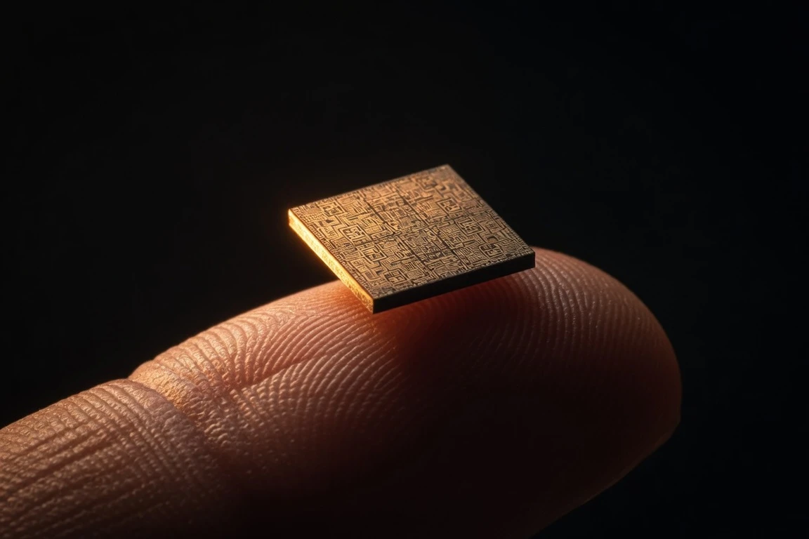
IBM unveiled what it calls the world’s first sub-1nm chip on June 25, 2026, a research-stage prototype built at the 0.7nm, or 7-angstrom, node. The fingernail-sized chip packs nearly 100 billion transistors using a new 3D architecture called nanostack. IBM framed the announcement as a milestone in extending the steady doubling of transistor counts that has powered decades of computing progress.
The chip is not a commercial product, and IBM is not a chipmaker. The company designs and prototypes transistors at research facilities in Albany, New York, then licenses the technology to foundries that handle mass production. The real test of the nanostack announcement is who builds it, and at what cost. IBM declined to name a manufacturing partner for the sub-1nm node.
What IBM Announced
IBM Research unveiled the chip from Yorktown Heights on June 25, 2026. The design sits at the 0.7nm, or 7-angstrom, node, where one angstrom equals one-tenth of a nanometer. IBM’s June 25 release on its sub-1nm chip says the prototype packs nearly 100 billion transistors into an area roughly the size of a fingernail, nearly twice the transistor density of its 2nm chip from 2021.
The breakthrough rests on what IBM describes as the industry’s first known 3D nanosheet-based transistor design. Instead of continuing to shrink transistors across a flat plane, the architecture vertically stacks and staggers them, using what IBM calls 3D sequential integration. Different materials can be used in each stacked layer, so engineers can tune performance and power efficiency in each transistor independent of the others. IBM says its semiconductor roadmap projects at least a decade of future scaling using the new architecture.
IBM’s latest chip breakthrough marks a landmark moment in computing, pushing technology beyond the nanometer era to the scale of atoms. With our new nanostack architecture, we’re not just making smaller transistors, we’re reinventing how chips are built to deliver dramatically more power and energy efficiency.
Jay Gambetta, director of IBM Research and an IBM Fellow, made the comment in IBM’s announcement. Node numbers in modern chips no longer describe actual transistor dimensions, and that detail matters for reading the announcement. Older generations of chips built in the 1970s and 1980s had physical features that matched the node number in their marketing names, but that has not been true for decades, Ars Technica’s reporting explains. Today, the 0.7nm label is a generational marker for a manufacturing process, not a literal measurement of transistor width. IBM itself makes this point clear in describing the angstrom era of chip development.
- 0.7nm (7 angstrom) node
- ~100 billion transistors per fingernail-sized chip
- up to 50% more performance vs 2nm
- up to 70% greater energy efficiency vs 2nm
- 40% SRAM scaling improvement
How Nanostack Works
Nanostack builds on nanosheet technology, the transistor architecture IBM invented in 2015 and that has since become the industry baseline. The basic unit of the new design consists of two transistors stacked and bonded together, the nanostack architecture described in detail. Each transistor contains three nanosheets individually 5 nanometers thick, roughly 15 rows of silicon atoms, with about 9 nanometers separating each sheet.
The mixed-material design is part of what makes nanostack different from previous generations. Because each stacked layer is built separately, engineers can mix and match different channel materials in each one. That allows the NFET and PFET channels to be optimized independently in a “gate stack” configuration. IBM Research says this staggered design improves cell layouts and shows a path toward even smaller nodes.
The work has been experimentally validated, not just modeled on paper. IBM researchers demonstrated functional CMOS inverter operation with expected switching performance, along with ultra-thin dielectric wafer bonding in CMOS integration. They also showed dual-channel engineering capability, confirming that nanostack can be physically built and supports real computation.
Published technical papers reported at the 2025 IEEE Symposium on VLSI Technology and Circuits in Kyoto laid out the underlying transistor architecture. The follow-up at the VLSI 2026 symposium added the SRAM scaling data. Together, the papers and presentations describe a research program that has produced working devices, not a finished manufacturing process.
In research presented at the VLSI 2026 symposium, the architecture delivered a 40% scaling improvement in SRAM, IBM’s biggest SRAM scaling gain in over a decade. SRAM, the fast but power-hungry on-chip memory that feeds AI workloads, had barely improved at all between the 3nm and 2nm generations, IBM’s own researchers noted. The gain came from a staggered-channel design for SRAM bit cells, the six-transistor memory units that hold bits on the chip. Reducing cell height by 40% lets designers pack more SRAM into the same footprint, which matters as on-chip memory bandwidth has become a known bottleneck for AI processors.
The Performance and Efficiency Numbers
IBM’s headline claim is a tradeoff between speed and power. The sub-1nm design can deliver up to 50% higher performance at the same power level as its 2nm chip, or up to 70 percent lower power consumption while maintaining the same performance. Published technical results reported at the VLSI 2025 symposium back the numbers. IBM framed both gains as projections from those results, not measurements of shipped products.
The 40% SRAM scaling improvement is the less-headline figure that may matter most for AI. SRAM is the on-chip memory that feeds data to processors, and shrinking SRAM cells has stalled in recent generations. IBM says the gain comes from a staggered-channel design that reduces SRAM cell height by 40%, allowing more memory per unit of chip area.
For AI specifically, IBM researchers estimated that accelerators built on the 7-angstrom process could deliver roughly 7,000 trillion operations per second, compared with about 1,500 TOPS for today’s leading AI accelerators. Training a frontier large language model that takes roughly three months on current hardware could drop to just a few weeks on 7-angstrom silicon, IBM projected. Those training-time figures are IBM’s own estimates, not measured benchmarks from third parties. The energy savings matter because AI data centers are straining electrical grids and hunting for water for cooling. A chip that does the same work for 70% less power attacks both problems at once.
| Attribute | IBM 2nm (2021) | IBM Sub-1nm (0.7nm / 7A) |
|---|---|---|
| Transistor count on fingernail-sized chip | Density baseline | nearly 100 billion |
| Density vs predecessor | Reference baseline | nearly 2x |
| Performance vs 2nm | Reference baseline | up to 50% higher |
| Energy efficiency vs 2nm | Reference baseline | up to 70% greater |
| SRAM scaling improvement | A few percent over 3nm | 40% |
| Manufacturing stage | In production via Rapidus, Samsung | Research prototype |
IBM Won’t Build These Chips
IBM’s enterprise partnerships reach beyond chips, but the company itself does not manufacture commercial chips. IBM designs and prototypes transistors at its research facilities and then licenses the technology to foundries. For its 2nm generation, IBM partnered with Rapidus in Japan to mass manufacture the chips and with Samsung in South Korea to commercialize related technology. None of those partners has been announced for the sub-1nm node.
IBM declined to name any specific companies that may partner with it to commercialize the newest sub-1nm technology. The announcement was framed as a research milestone, not a commercial product. Whoever picks up the architecture will have to build out the new manufacturing process from the ground up.
Huiming Bu, vice president of IBM Semiconductors Global R&D and IBM Research, expects commercial chips at the sub-1nm node to begin production as early as in the next five years and most likely within a decade. “It will replace nanosheet as today’s mainstream in leading foundries, whether it’s CPUs or GPUs,” Bu said in the media briefing. “Within a decade, this will become another mainstream that we have invented and helped industry to transform.” Nanosheet, the architecture nanostack builds on, is now “adopted by all leading foundries for most of the 3-nanometer chips and all of the 2-nanometer chips,” per Bu.
TSMC, the world’s largest contract chipmaker, is ramping production of its 2nm process technology using first-generation nanosheet transistors. The Taiwanese company is also developing its A16 and A14 next-generation manufacturing technologies on its own roadmap. Intel has its own 18A and 14A nodes in development, with 14A targeting the 1.4nm-class range on its public roadmap. Each of those programs is using nanosheet-derived designs, which means nanostack is competing to be the architecture that replaces nanosheet rather than one that arrives before it. The architectural race is now between IBM’s 3D stacking and the rest of the industry’s 2D refinements.
The Five-Year-to-a-Decade Roadmap
Other major computing roadmaps have pegged similar five-to-seven-year timelines, and IBM’s nanostack schedule sits in the same range. IBM sees a path to production in as early as the next five years, with the technology becoming mainstream within a decade. Huiming Bu projects that within a decade, nanostack will replace nanosheet as the leading-edge architecture.
The roadmap depends on toolchain partners IBM has already named. ASML is supplying a High Numerical Aperture Extreme Ultraviolet lithography tool that will be installed at IBM’s Albany, New York research facility. Lam Research, Tokyo Electron, and SCREEN Semiconductor Solutions are co-developing the High NA EUV processes around that tool. IBM said the work has already produced functioning devices, though those are research demonstrations, not production chips.
To put the scale into perspective, IBM Research’s scale comparison of the 7-angstrom node notes a human red blood cell is about 7,000 nanometers wide, roughly 10,000 times larger than the chip’s 0.7nm transistor node. IBM says the announcement marks the beginning of what it calls the angstrom era, where transistor dimensions are measured in angstroms rather than nanometers. One angstrom equals one-tenth of a nanometer. The “angstrom era” framing is IBM’s own marketing language, not an industry-wide standard term. Roadmap specifics beyond the next decade have not been made public.
Stock Reaction
Investors read the announcement as a positive signal. IBM shares rose about 5% in premarket trading on June 25, 2026, according to multiple market reports. The move came on a broader day of chip-sector volatility, with Micron’s earnings report also driving the semiconductor complex. By the close, IBM shares had given back part of the premarket gain.
The market response reflected a research milestone with a long tail, not an imminent revenue event. IBM described the announcement as a research achievement, not a shipping product. Commercial chips at the sub-1nm node are at least five years away, per IBM’s own timeline. Whoever licenses nanostack for production will need to build out a new fabrication process, and IBM has not said which foundry will take it. The chip news is real, and the partner question remains open.
Frequently Asked Questions
What is IBM’s sub-1nm chip?
The 0.7nm (7 angstrom) chip IBM unveiled on June 25, 2026 is a research-stage prototype that packs nearly 100 billion transistors in a fingernail-sized area, roughly twice the density of IBM’s 2nm chip from 2021.
How does the nanostack architecture work?
Nanostack vertically stacks and staggers transistors in two layers on a silicon chip using 3D sequential integration. Different materials can be used in each layer, letting NFET and PFET channels be tuned independently for performance and power.
When will sub-1nm chips reach products?
IBM projects the earliest commercial adoption could begin in the next five years, with the technology becoming mainstream within a decade. The timeline is IBM’s own projection, not a confirmed shipping date from any foundry partner.
Who will manufacture sub-1nm chips?
IBM has not announced a manufacturing partner for the sub-1nm node. The company does not operate commercial fabs and has previously partnered with Rapidus in Japan and Samsung in South Korea for its 2nm generation, but neither has been named for sub-1nm production.
How does this compare to TSMC, Intel, and Samsung roadmaps?
TSMC is ramping its 2nm process using first-generation nanosheet transistors and developing A16 and A14 nodes. Intel has 18A and 14A on its public roadmap, with 14A targeting the 1.4nm-class range. IBM’s claim is that nanostack will replace nanosheet as the leading architecture within a decade.


T-Mobile’s Free iPhone 17 Deal Carries a 24-Month String

Nvidia’s AI Security Alliance Excludes OpenAI, Google and Anthropic

CleanMy®Phone Clears iPhone Clutter and Funds Ukraine’s Defense

Amodei Rejects Open-Weight AI Ban, Pushes Chip and Distillation Curbs

Americans Say China Leads AI While the Money Still Says Otherwise

ONR Bets on AI to Run Research and Multiply Program Officers

TrendAI Appoints Richard Harrison as First Auckland-Based Global VP

Honor’s Robot Phone Launches August 12 as IPO Pressure Builds

The Snapdragon 8s Elite Leak That Foreshadowed Qualcomm’s Chip Split

Ookla’s Manila Study Favors Carrier Calls as Philippines’ 3G Deadline Nears

Fable 5 and Mythos 5 Return as US Lifts Anthropic Export Controls

SpaceX’s Google Deal Turns a Rocket Company Into a Cloud Landlord

CD Projekt Red Co-CEO: Redemption Arc Isn’t Done, Witcher 4 in 2027

Oracle Cuts 21,000 Jobs in a Year, Cites AI in 10-K Filing

XPL Rallies 30% Ahead of Plasma One Card Tier Launch

DGO App Brings Rs 549 Mobile Pass for FIFA World Cup 2026 in Nepal

Google Search Profiles Build a Follow Graph Inside Discover

Moonshot AI Targets $30 Billion in China’s Fastest AI Funding Sprint

Microsoft Xbox Layoffs Start in July as Sharma Slams 3% Margin

Oppo’s ColorOS 17 Eligibility List Leaves A-Series Buyers Behind
-
 AI4 weeks ago
Fable 5 and Mythos 5 Return as US Lifts Anthropic Export Controls
-
 AI2 months ago
SpaceX’s Google Deal Turns a Rocket Company Into a Cloud Landlord
-
 GAMING1 month ago
CD Projekt Red Co-CEO: Redemption Arc Isn’t Done, Witcher 4 in 2027
-
 AI1 month ago
Oracle Cuts 21,000 Jobs in a Year, Cites AI in 10-K Filing
-
 CRYPTO2 months ago
XPL Rallies 30% Ahead of Plasma One Card Tier Launch
-
 APPS2 months ago
DGO App Brings Rs 549 Mobile Pass for FIFA World Cup 2026 in Nepal
-
 NEWS2 months ago
Google Search Profiles Build a Follow Graph Inside Discover
-
 AI2 months ago
Moonshot AI Targets $30 Billion in China’s Fastest AI Funding Sprint