AI
ASE Technology Says AI Chip Demand Is Now the Bottleneck
ASE Technology is breaking ground on six new plants in 2026 and targeting $3.2B in advanced packaging as AI demand from Nvidia, AMD, and Amazon tightens supply.
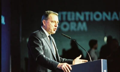
ASE Technology Holding is expanding capacity to handle surging demand for AI chips, Chief Operating Officer Tien Wu said this week, a buildout that includes six new factories breaking ground worldwide in 2026 and a target of advanced packaging sales roughly doubling to $3.2 billion this year. The Taiwanese company, the world’s largest chip packager and tester, said the scale of construction in 2026 will be the largest single year in its history, and that co-packaged optics will enter volume production for the first time. Tien Wu framed the moment bluntly in remarks to media in Kaohsiung: hardware supply has become the bottleneck for AI, and the company intends to keep building to clear it.
Most coverage of the AI buildout stops at the names on the chip: Nvidia, AMD, Amazon. The company that actually puts those AI accelerators into a final, shippable package is rarely named. That is the gap Tien Wu is filling, and the gap he expects to grow. “The simultaneous groundbreaking of six new plants this year sets a record for the largest single-year construction scale in the company’s history,” he said at the Renwu groundbreaking in Kaohsiung on April 10, 2026.
Tien Wu Says Capacity Has Become the AI Bottleneck
ASE is the largest pure-play chip packager in the world, with consolidated 2025 revenue of NT$645,388 million (US$20,782 million) and an assembly, testing, and materials (ATM) business that grew 19.4% year on year. The ATM unit is now the company’s growth engine, and AI is the engine inside the engine.
Tien Wu told media that the demand for advanced packaging is still in its infancy, and that the current AI buildout is only the first wave of a multi-wave cycle. “We are confident about AI demand over the next decade, while hardware supply has become the bottleneck now,” he said, adding that the company will keep raising its capital spending to keep up. The framing matters: ASE is not pitching a one-time ramp. It is committing to a multi-year capacity build, with capex scaling above the US$5.5 billion it spent in 2025.
Six New Plants Breaking Ground in 2026, the Largest Construction Year in ASE’s History
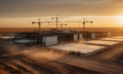
The most concrete piece of the build is the new Renwu cluster in Kaohsiung, where ASE, partner WinWay Technology, and automation supplier HORNG TERNG broke ground on April 10, 2026. The site will integrate AI-driven smart manufacturing, including visual cloud inspection systems and fully automated guided vehicles, and is designed to meet Kaohsiung’s green-building standards.
The Renwu project alone commits over NT$108.3 billion in capital investment and targets projected annual output of approximately NT$177.3 billion once fully operational, according to the company’s April 10, 2026 groundbreaking press release. The complex is expected to create over 1,000 jobs. Phase I is scheduled to begin operations in April 2027, with Phase II following in October of the same year. The Renwu site is part of Kaohsiung’s Southern Semiconductor S Corridor, an industrial plan the city government is using to position the south of Taiwan as a hub for silicon photonics and advanced packaging.
Renwu is one of six new plants breaking ground globally in 2026, a buildout Tien Wu said is the largest single-year construction scale in the company’s history. Each site targets different pieces of the AI supply chain, from advanced packaging to high-end testing.
| Project | Location | Capital investment | Targeted output | Operating timeline |
|---|---|---|---|---|
| Renwu hi-tech testing cluster | Kaohsiung, Taiwan | Over NT$108.3 billion | Approximately NT$177.3 billion annual output | Phase I April 2027, Phase II October 2027 |
| Penang P5 advanced packaging plant | Penang, Malaysia | Per ASE Penang launch announcement | Advanced packaging and testing capacity | Fifth Malaysia plant; expanding existing campus |
| Four additional global plants (combined) | Worldwide, including Korea and the Philippines | Part of 2026 capex above the $5.5B 2025 base | LEAP advanced packaging and high-end test | All breaking ground in 2026, per Tien Wu |
The spending plan underpinning the six-plant build was laid out in EE Times’ report on ASE’s 2026 advanced-packaging target, which noted that ASE will increase its 2026 capital expenditure by an undisclosed amount from the $5.5 billion spent in 2025 and is buying cleanrooms and building its own to expand into advanced packaging. The company also said co-packaged optics (CPO) will enter volume production for the first time this year, a milestone Tien Wu characterized as the rise of optical communication being an undeniable trend.
What’s Going Inside Those New Plants
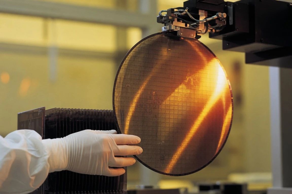
Advanced packaging is the back-end step that takes finished silicon dies and assembles them into a single working chip, a stage that has become the rate-limiter for AI accelerators. Older packages held one die. Modern AI parts stack multiple dies side by side or on top of each other and connect them with thousands of tiny wires, so the silicon can think in parallel without burning the budget on a single massive die.
CoWoS, or chip-on-wafer-on-substrate, is the most common family of these 2.5D techniques, and it is what Nvidia, AMD, and most of the AI accelerator market use. ASE’s LEAP, or Leading Edge Advanced Packaging, line is its portfolio of these techniques, and the company is targeting roughly a doubling of LEAP revenue to US$3.2 billion in 2026, per EE Times’ report on ASE’s packaging and testing strategy.
Inside the new plants, three technical threads are running at once.
- CoWoS and CoWoS-L advanced packaging for high-bandwidth memory stacks and AI accelerators, the work ASE has been winning from TSMC’s outsourcing pipeline.
- Co-Packaged Optics (CPO) entering volume production for the first time, replacing traditional pluggable optical modules with optics that sit on the same package as the switch ASIC, cutting power and raising bandwidth. Tien Wu said the rise of optical communication is an undeniable trend, and CPO is the form factor that trend takes.
- AI-driven smart manufacturing, including the visual cloud inspection systems and fully automated guided vehicles ASE said will run the Renwu plant.
- Green-building compliance under the Kaohsiung Green Building Autonomy Ordinance, the regulatory hook that turns the new fabs into a proving ground for low-carbon semiconductor manufacturing.
The new tools matter because older OSAT, or outsourced semiconductor assembly and test, lines are full. “Our ATM factories in Taiwan ran at or near full capacity with LEAP and traditional advanced packaging utilization rates outpacing that of wirebond,” Tien Wu said on ASE’s Q4 2025 earnings call, in ASE’s Q4 2025 earnings-call coverage. The build is, in effect, a bet that AI demand holds long enough to fill the new lines as they come online, and the demand side of that equation is the one with the most moving parts.
The Customers Behind ASE’s Buildout
The customers are the same names that dominate every AI buildout story, and they are the reason ASE is building. Nvidia is the anchor, with subsidiary SPIL participating in Nvidia’s US$500 billion Arizona AI infrastructure build over the next four years. AMD is the second leg, with JPMorgan analyst Gokul Hariharan projecting that AMD’s Venice CPUs will be the first products to use ASE’s full-process packaging, starting in the second half of 2026.
Amazon is the third. Hariharan’s February 6, 2026 report, cited in EE Times’ coverage, projected AMD could bring $300 million to $400 million in revenues to ASE in 2026, with further room for growth in 2027 as multiple non-GPU AMD products move to ASE’s 2.5D process. The same report flagged potential share gains in Amazon’s Trainium3 ASICs and said ASE could see Nvidia Vera CPU outsourcing in 2027. That sequence, Nvidia GPU first, AMD CPU second, Amazon ASIC third, is the demand profile the six new plants are being sized to serve.
TSMC’s Monopoly on Advanced Packaging Is Cracking
The structural shift making ASE’s buildout possible is happening upstream, at the world’s largest foundry. TSMC has effectively owned advanced packaging for the AI cycle, and it is now ceding the on-substrate work to the OSATs.
JPMorgan’s Gokul Hariharan framed the shift in his February 6, 2026 report. “In 2026, we believe that the primary driver for growth is likely to be on-substrate outsourcing from TSMC for Nvidia GPUs, with a meaningful step up likely in second-half 2026 as [Nvidia] Rubin GPUs start ramping,” he said. The reason is straightforward: TSMC has budgeted a record $52 billion to $56 billion in capital expenditure this year and still cannot keep up with AI chip demand. Outsourcing is the relief valve.
ASE is positioned to take the largest share of that work. Its 2.5D capacity, its existing relationships with Nvidia and AMD, and the SPIL footprint in Arizona all make it the default second source.
It is our feeling that the demand for advanced packaging [technologies] is still in its infancy, as this AI [demand] is just the first wave, which will be followed by a second and third wave.
Tien Wu, Chief Operating Officer of ASE Technology Holding, said the same in a media briefing in Kaohsiung, in remarks reported by the Taipei Times in 2025. At the company’s April 2026 Supplier Day, the longer-horizon framing went even further. “Driven by surging demand for AI and High-Performance Computing (HPC), the global semiconductor industry is projected to exceed US$1 trillion by 2026, reflecting strong structural growth,” Tien Wu told over 100 global partners, per the ASE April 2026 Supplier Day briefing. He added that the industry has elevated hardware’s role from a mere component to a defining factor in enabling innovation at scale, language that doubles as a forecast and a defense of the multi-year capex commitment the six-plant buildout represents.
The Risks Hiding Under the Buildout
The bet has costs, and the first is the capex bill itself. ASE’s 2025 ATM capex was roughly $2.5 billion, up about 32% from 2024’s $1.9 billion, and the 2026 step-up takes total capital spending above the US$5.5 billion consolidated base. The company has signaled that the initial 2026 capex still has room for upward revision, with the specifics to be disclosed at its next investor briefing.
The second risk is the US tariff overhang. Tien Wu said the US tariff policy carries weight with ASE’s global manufacturing deployments, and that the company is closely monitoring how the tariff landscape is evolving before making any capacity adjustments. Taiwan was negotiating to reduce a proposed 32% reciprocal tariff in 2025, and the outcome of those talks will decide how aggressive ASE’s US footprint becomes. A made-in-America OSAT line is technically viable, Tien Wu said, but requires customer support, employee readiness, and a willingness to duplicate manufacturing technologies in an unfamiliar country.
The third risk is supply-chain stress, including power and components, that comes with building six new plants at once. Andrew Tang, ASE’s Chief Procurement Officer, said the company is seeing heightened supply-demand volatility, extended lead times, and an accelerated pace of technology advancement across its supplier base, the same pressures that pushed ASE to convene over 100 partners at its April 2026 Supplier Day. A separate Goldman Sachs note on Taiwan power-supply chain, captured in Goldman’s April 2026 call on AI power supplier Delta Electronics, shows the same dynamic on the power side: AI infrastructure is pushing every adjacent component category into shortage.
For 2026, the data points worth tracking are the new Renwu lines coming online in 2027, the second-half 2026 ramp of Nvidia Rubin packaging, and the company’s next investor briefing, where Tien Wu said the 2026 capex revision will be disclosed.
- US$3.2 billion – ASE’s 2026 LEAP advanced packaging revenue target
- US$5.5 billion – ASE’s 2025 capital expenditure, the base from which 2026 is being raised
- NT$108.3 billion – Renwu plant capital investment (Kaohsiung)
- NT$177.3 billion – Renwu’s projected annual output at full operation
- 1,000+ – jobs the Renwu cluster is expected to create
Frequently Asked Questions
What is ASE Technology Holding?
ASE Technology Holding Co., Ltd. (TWSE: 3711, NYSE: ASX) is the world’s largest outsourced chip packaging and testing provider, and the parent of subsidiaries including ASE, SPIL, and USI. The company reported NT$645,388 million (US$20,782 million) in 2025 consolidated revenue and is headquartered in Kaohsiung, Taiwan.
What does “advanced packaging” mean, and why does it matter for AI?
Advanced packaging is the back-end step that assembles multiple finished silicon dies into a single working chip. The dominant family is CoWoS, or chip-on-wafer-on-substrate, the technique behind most AI accelerators. It is the rate-limiter for AI chip supply because the front-end fabs can already make the dies; the back-end lines are what cannot keep up.
Why is TSMC outsourcing to ASE?
TSMC has struggled to keep up with AI chip demand even as it has budgeted a record $52 billion to $56 billion in capital expenditure this year, and is likely to transfer more of the on-substrate work to outsourced assembly-and-test companies, per JPMorgan’s Gokul Hariharan in his February 6, 2026 report. ASE is the largest of the OSATs positioned to take that work.
How much is ASE spending on the expansion?
ASE said it will increase 2026 capital expenditure by an undisclosed amount from the $5.5 billion it spent in 2025. The Renwu cluster alone commits over NT$108.3 billion in capital investment, with phase one scheduled to begin operations in April 2027.
What does ASE expect to deliver in 2026?
Advanced packaging, or LEAP, revenue is targeted to roughly double in 2026 to US$3.2 billion, and co-packaged optics (CPO) is set to enter volume production for the first time. Tien Wu has said the initially planned annual capex still has room for upward revision, with the specifics due at the next investor briefing.

Alibaba’s Qwen3.8 Max Challenges a Rival It Helped Fund

Google and Apple’s EU AI Warnings Echo Meta’s WhatsApp Fight

FIFA World Cup 2026 Fraud Followed Qatar 2022’s Playbook Into Offices

POCO M8 Power’s Flipkart Tease Exposes Xiaomi’s Rebadge Playbook

Elekta’s Profit Beat Couldn’t Stop a 14% Stock Selloff

Supply Chain Hack Defenses Now Rest on a Handful of Tech Giants

Battlefield 6’s Top Gun Crossover Breaks the Promise DICE Made by Name

Hugging Face Turned to a Chinese AI Model When American Ones Refused

HP’s OmniBook Ultra 14 Review Puts Intel’s Comeback Bet to the Test

India May Dodge Apple’s iPhone Price Hike, but Not Forever

SpaceX’s Google Deal Turns a Rocket Company Into a Cloud Landlord

DGO App Brings Rs 549 Mobile Pass for FIFA World Cup 2026 in Nepal

XPL Rallies 30% Ahead of Plasma One Card Tier Launch

Google Search Profiles Build a Follow Graph Inside Discover

CD Projekt Red Co-CEO: Redemption Arc Isn’t Done, Witcher 4 in 2027

Oracle Cuts 21,000 Jobs in a Year, Cites AI in 10-K Filing

Moonshot AI Targets $30 Billion in China’s Fastest AI Funding Sprint

Fable 5 and Mythos 5 Return as US Lifts Anthropic Export Controls

Microsoft Xbox Layoffs Start in July as Sharma Slams 3% Margin

WhatsApp Meta Business Agent Reaches India, With a New Pricing Meter
-
 AI1 month ago
SpaceX’s Google Deal Turns a Rocket Company Into a Cloud Landlord
-
 APPS1 month ago
DGO App Brings Rs 549 Mobile Pass for FIFA World Cup 2026 in Nepal
-
 CRYPTO1 month ago
XPL Rallies 30% Ahead of Plasma One Card Tier Launch
-
 NEWS1 month ago
Google Search Profiles Build a Follow Graph Inside Discover
-
 GAMING4 weeks ago
CD Projekt Red Co-CEO: Redemption Arc Isn’t Done, Witcher 4 in 2027
-
 AI4 weeks ago
Oracle Cuts 21,000 Jobs in a Year, Cites AI in 10-K Filing
-
 AI1 month ago
Moonshot AI Targets $30 Billion in China’s Fastest AI Funding Sprint
-
 AI3 weeks ago
Fable 5 and Mythos 5 Return as US Lifts Anthropic Export Controls