AI
Sandisk’s High Bandwidth Flash Takes Aim at the AI Memory Wall
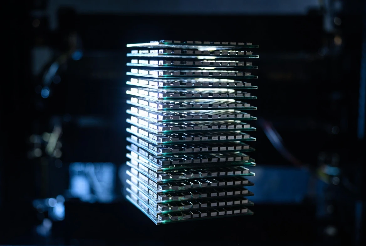
Sandisk’s High Bandwidth Flash is a NAND-based memory tier designed to sit beside AI accelerators. SK hynix, the HBM market leader, is co-writing the spec.
Sandisk and SK hynix have begun writing the specification for High Bandwidth Flash (HBF), a NAND-based memory tier the two companies are pitching as the first purpose-built answer to AI inference’s capacity wall. The 25 February 2026 kickoff at Sandisk’s Milpitas headquarters sits inside a dedicated workstream under the Open Compute Project, the standards body that has hosted most of the data centre’s open hardware specs.
The announcement reframes the AI memory stack. Today’s data centres bolt DRAM or specialised high-bandwidth memory (HBM, stacked DRAM dies that sit beside the GPU and feed it data at high bandwidth) onto AI accelerators, and HBF targets that exact tier with NAND flash instead. Sandisk’s chief technology officer, Alper Ilkbahar, called the work “setting the bar for the next era of AI computing,” and SK hynix is at the same table even though it holds the largest share of the HBM market.
The Memory Wall Started Cracking When Inference Became the Workload
For two decades, the data centre’s memory hierarchy was built for general-purpose computing, and DRAM plus HBM made it work. AI training fits the model: you load weights into HBM, train, write the weights back, repeat. Inference runs differently. It runs continuously as a deployed model generates answers for millions of users at once, and the live model has to sit beside the compute because every token pulls from the same weights.
Sandisk’s framing of the problem, drawn from its August 2025 collaboration announcement with SK hynix, runs through three fault lines DRAM and HBM cannot close: capacity at the inference tier, density per square millimetre, and cost per terabyte at scale. A fourth issue compounds the first three. DRAM needs constant refreshes to keep its bits, which costs power and creates a thermal ceiling as inference clusters grow.
Inference models also do not use DRAM’s strongest property. The access patterns of LLM inference are deterministic, which means data can be prefetched ahead of time, and the latency advantage DRAM offers matters far less than the bandwidth the model can pull from its memory. Paying for the lowest-latency memory in a workload that does not use the lowest-latency layer is the structural gap HBF is built to fill.
What HBF Is, Stack by Stack
HBF is NAND flash stacked 16 dies high on Sandisk’s BiCS architecture, with the company’s CBA (CMOS-bonded-array) wafer bonding doing the package-level work. The result is a memory module built into an HBM-compatible physical footprint, so it drops into existing accelerator designs without remaking the rest of the system.
On the spec sheet, the first-generation stack holds 512GB and matches HBM4’s footprint, power profile, and stack height, per Sandisk’s own technical write-up. Sandisk also says first-generation HBF delivers up to 8x to 16x the capacity of an equivalent HBM stack at a similar cost, with comparable bandwidth. Because the underlying storage is NAND, HBF retains its data when powered down and stays stable at higher operating temperatures than DRAM.
| Spec | What Sandisk publishes for first-generation HBF |
|---|---|
| Capacity per 16-die stack | 512GB |
| Capacity vs HBM | Up to 8x to 16x at similar cost |
| Bandwidth vs HBM | Comparable bandwidth |
| Physical package | HBM4-compatible footprint, power profile, stack height |
| Persistence | Non-volatile; retains data when powered down |
The trade-off is the one anyone familiar with NAND expects: flash latency sits higher than DRAM. For streaming large model weights that is tolerable; for latency-critical random access it is not, which is exactly why Sandisk pitches HBF as an inference complement rather than a DRAM replacement.
A Turing Laureate Chairs the Board
A single vendor announcing a new memory standard is a press release. Sandisk added weight to HBF in July 2025 with the formation of its HBF Technical Advisory Board. The board is chaired by David Patterson, the emeritus Pardee Professor of Computer Science at the University of California, Berkeley, and a Google distinguished engineer.
HBF shows the promise of playing an important role in datacenter AI by delivering unprecedented memory capacity at high bandwidth, enabling inference workloads to scale far beyond today’s constraints. It could drive down costs of new AI applications that are currently unaffordable.
Patterson co-developed Reduced Instruction Set Computing (RISC), the design philosophy most modern CPU cores use, and the Redundant Array of Inexpensive Disks (RAID) storage model. The ACM awarded him its 2017 Turing Award, computer science’s closest equivalent to a Nobel. Joining him is Raja Koduri, founder and CEO of Oxmiq Labs, and the former Senior Vice President and Chief Architect at AMD, and Executive Vice President of Accelerated Computing Systems and Graphics at Intel. Koduri directed the development of AMD’s Polaris, Vega, and Navi GPU architectures, and Intel’s Arc and Ponte Vecchio GPUs.
Koduri’s quote on HBF focused on the edge: “HBF is set to revolutionize edge AI by equipping devices with memory capacity and bandwidth capabilities that will support sophisticated models running locally in real time.” That is the second reason the advisory board matters. Sandisk is pitching HBF for hyperscale and for phones and edge boxes, and Koduri’s background in consumer graphics is the rare credential set that touches both worlds.
The HBM Leader Sitting at the Same Table
SK hynix led the global HBM market with 57% of revenue in the third quarter of 2024, per Counterpoint Research data reported in a January 2026 SK Hynix profit lead report. SK hynix is now co-authoring an HBF specification that targets its own franchise.
The framing from SK hynix president and chief development officer Ahn Hyun, in the August 2025 memorandum announcement, runs through standardisation: “Through our work with Sandisk to standardize the High Bandwidth Flash specification, we are actively contributing to the commercialization of this innovative technology.” Ilkbahar’s framing runs through demand: “By collaborating with SK hynix to define the High Bandwidth Flash specification, we are addressing the critical need for scalable memory in the AI industry.” The Open Compute Project workstream that started on 25 February 2026 is the entry point, binding SK hynix’s NAND packaging expertise to Sandisk’s HBF design. Once the spec exists, any foundry with a NAND process can build to it, which is the concrete mechanism the standard opens up beyond the two companies sitting at the table.
Incumbents Are Quietly Hedging
The HBM market did not stand still while HBF was being designed. Counterpoint’s MS Hwang told CNBC he expects Samsung to “show a significant turnaround with HBM4 for Nvidia’s new products” in 2026, moving past last year’s quality issues, and Samsung has said it remains on track to begin delivering HBM4 this year. SemiAnalysis analyst Ray Wang, also cited by CNBC, framed the HBM4 generation as “really between SK Hynix and Samsung,” with both more competitive than Micron.
HBM4 raises the HBM bar but leaves the same structural gap. It makes the HBM stack faster and denser on a per-stack basis the DRAM industry knows how to price. Inference models want comparable bandwidth with more capacity per dollar, the metric Sandisk’s 8x to 16x capacity claim targets. The two product families can sit side by side. They are pointed at slightly different lines inside the same hyperscaler budget.
Sandisk’s share price has already moved on AI storage demand. The stock jumped 55% in May 2026, per a recent piece on the 1990s-tech-stock re-rating.
When the Parts Ship, and What They Reach
Sandisk has set a public timeline for HBF. First samples of the memory ship in the second half of 2026, with the first AI-inference devices carrying the parts expected in early 2027, per the company’s August 2025 release. The Open Compute Project workstream that started on 25 February 2026 standardises the spec, not the silicon, so the timeline for true hyperscale deployments sits further out, behind the 2027 inference platforms that adopt the new memory tier.
When HBF lands, the immediate impact is on cost per gigabyte of inference memory, not on raw latency. Inference clusters that need 4TB of model weights beside a single accelerator cannot afford that capacity in HBM today. Because HBF persists when power drops and tolerates higher heat than DRAM, it also opens edge AI devices, including phones and small inference boxes HBM cannot reach on cost or thermal grounds, and it lets those devices carry long context across power cycles without round-tripping to a cloud.
Sandisk’s blog on the technology, written by Ilkbahar, ties HBF’s simulated bandwidth to a real model. In the company’s reading of the Llama 3.1 405B model on simulated HBF, reading pretrained weights landed within 2.2% of a hypothetical, unlimited-capacity HBM baseline, the figure in Sandisk’s technical write-up on the HBF memory wall problem. Sandisk frames that gap as closable. The field will judge it when the silicon comes back from the fab.
Frequently Asked Questions
What is Sandisk’s High Bandwidth Flash?
High Bandwidth Flash (HBF) is a NAND flash memory stack built to sit beside AI accelerators in the same physical slot as HBM, with comparable bandwidth and up to 16x the capacity at a similar cost, according to Sandisk’s August 2025 collaboration announcement with SK hynix.
Is HBF a replacement for HBM or DRAM?
No. Sandisk and SK hynix pitch HBF as a complement to HBM, not a substitute. Flash latency sits higher than DRAM, which makes HBF best suited to streaming large model weights for inference rather than the latency-critical random access that needs DRAM-grade memory.
When will HBF samples ship?
Sandisk says first samples of HBF memory arrive in the second half of calendar 2026, with the first AI-inference devices carrying HBF expected in early 2027. The Open Compute Project workstream that kicked off on 25 February 2026 covers the specification, not the silicon.
Who is David Patterson and why does his endorsement of HBF matter?
Patterson is the emeritus Pardee Professor of Computer Science at the University of California, Berkeley, and a Google distinguished engineer. He co-developed RISC and RAID, and won the 2017 ACM Turing Award. He chairs Sandisk’s HBF technical advisory board, lending institutional weight to a memory standard that launched from a single vendor.
Why is SK hynix helping standardise a memory that could compete with HBM?
SK hynix led the global HBM market with 57% of revenue in the third quarter of 2024, per Counterpoint research cited by CNBC. Helping write the HBF specification puts the company’s NAND packaging expertise to work in a category adjacent to HBM, and gives the HBM leader a seat at the table for whatever the next AI memory tier looks like.

LexisNexis and Promon Pair Up to Catch Mobile Fraud Inside the App

Five Channel Islands Experts on Why Technology Alone Falls Short

Gartner Warns $234 Billion in SaaS Spend Faces Agentic AI Reshuffle

Logitech G Becomes Modern Warfare 4’s Official PC Peripheral Partner

Sony PlayStation Handheld Rumors Reignite After Nishino Q&A

Huawei’s Standard Mate 80 Tops H1 2026 Sales, Pro Max Trails

SMS Authentication Is Failing Australian Mortgage Brokers

WiseTech’s 32-Year Data Trove Is Now Its Logistics AI Edge

Samsung Unpacked July 22 Confirmed by Members App Voucher Leak

A $6.99 Manga Subscription Just Pooled 10-Plus Publishers

Google Search Profiles Build a Follow Graph Inside Discover

Microsoft Xbox Layoffs Start in July as Sharma Slams 3% Margin

Google DeepMind and A24 Sign $75 Million AI Partnership Deal

Apple Strikes Preliminary Deal For Intel To Make iPhone And Mac Chips

DGO App Brings Rs 549 Mobile Pass for FIFA World Cup 2026 in Nepal

Anthropic Tells Senators Alibaba Ran the Largest Claude Distillation Attack

VinRobotics’ VR-H3 Debuts at Vienna, VinFast Is Next

Andreessen Horowitz Bets $2.2B on Crypto’s Quiet Cycle

Oracle Cuts 21,000 Jobs in a Year, Cites AI in 10-K Filing

Oppo’s ColorOS 17 Eligibility List Leaves A-Series Buyers Behind
-
 NEWS4 weeks ago
Google Search Profiles Build a Follow Graph Inside Discover
-
 GAMING3 weeks ago
Microsoft Xbox Layoffs Start in July as Sharma Slams 3% Margin
-
 AI1 week ago
Google DeepMind and A24 Sign $75 Million AI Partnership Deal
-
 NEWS2 months ago
Apple Strikes Preliminary Deal For Intel To Make iPhone And Mac Chips
-
 APPS3 weeks ago
DGO App Brings Rs 549 Mobile Pass for FIFA World Cup 2026 in Nepal
-
 AI1 week ago
Anthropic Tells Senators Alibaba Ran the Largest Claude Distillation Attack
-
 AI4 weeks ago
VinRobotics’ VR-H3 Debuts at Vienna, VinFast Is Next
-
 CRYPTO2 months ago
Andreessen Horowitz Bets $2.2B on Crypto’s Quiet Cycle