
COMPUTERS
Huawei Bets on Folded Logic to Chase TSMC’s 1.4nm by 2031

Huawei used a Shanghai conference stage on May 25 to put a number on the wall: transistor density equivalent to 1.4-nanometer chips by 2031, built without a single extreme ultraviolet (EUV, the lithography class US sanctions block Chinese buyers from owning) machine on its foundry partner’s floor. TSMC’s own A14 process roadmap puts the same milestone in mass production in the second half of 2028, three years earlier.
That 1.4nm-equivalent line rests on a five-letter qualifier the press releases skipped past. Matching density on paper is one engineering problem. Matching yield, power, cost, and design-tool ecosystem is a different set of problems, and the autumn launch of the next Kirin processor will tell readers more about where Huawei sits today than any conference slide can.
What Huawei Put on the ISCAS Stage
He Tingbo, chairwoman of Huawei’s Scientist Committee and president of the company’s semiconductor business, delivered a keynote at the 2026 IEEE International Symposium on Circuits and Systems titled New Semiconductor Path in Practice. The pitch had two pieces: a new scaling framework Huawei calls the Tau (τ) Scaling Law framework, and a circuit-design technique called LogicFolding that Huawei says implements it.
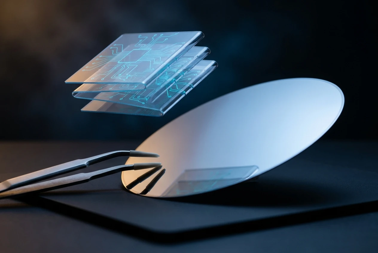
The Tau idea swaps the industry’s geometric scaling target (smaller feature sizes) for a temporal one (shorter signal propagation time). Designers optimize for how fast electrons cross a chip rather than how tightly transistors pack together. LogicFolding then stacks logic layers physically so the wires connecting them shrink in length, which the company says reduces resistive and capacitive load on critical paths.
Four numbers anchored the keynote:
- 55% higher transistor density than a comparable un-folded design
- 41% better power efficiency over the same baseline
- 381 chips designed and mass-produced over six years using these principles
- 1.4nm-equivalent density target for high-end silicon by 2031
Commercially, Huawei said the Mate 90 series Kirin processor launching this autumn will be the first product to fully adopt LogicFolding. Scaling the architecture into Ascend AI processors and data-center silicon is targeted for 2030. SMIC, China’s largest foundry and Huawei’s main manufacturing partner, is the line that has to make the math work.
The Word “Equivalent” Carries the Argument
Here is what the 2031 number does not say. Transistor density is one of several axes a process node is judged on. The others are yield (the share of dies on a wafer that come out functional), power efficiency at sustained load, defect density, manufacturing cost per wafer, and the maturity of the EDA (electronic design automation, the software toolchain designers use) ecosystem around the node.
A folded-logic design fabricated on a mature DUV (deep ultraviolet) process can hit the gate count of a smaller node on a die-shot. Whether it hits the yield and cost of that node is a different conversation, and the experience curve favors whoever has spent a decade refining the underlying process.
TechInsights, the chip-analysis firm that x-rays packaged silicon for a living, has been clear that SMIC’s current N+3 process is closer to a tight 7nm than to a true 5nm. Its analysts have flagged that the multi-patterning techniques pushing N+3 past 7nm equivalence carry a wafer-cost penalty and a defect-rate penalty that scale unfavorably as features shrink.
That cost penalty matters when the comparison is to a 1.4nm-class wafer produced with EUV and, eventually, high-NA EUV. A folded 14-nanometer stack and a true 1.4nm transistor can plot at the same gates per square millimeter and still belong in different commercial categories. The folded version runs hotter at scale and leans harder on packaging and thermal solutions that themselves eat margin.
None of this makes the Tau framework irrelevant. It does mean that “equivalent density” is a marketing line aimed at the gap narrative, and the engineering line a serious investor should read is whether per-wafer cost and yield curves on folded logic bend the right way in the next two product cycles.
SMIC Starts the Race From N+3
The starting position matters. The most advanced shipping node in China is SMIC’s N+3, a scaled extension of its 7nm-class N+2 process, and it is the node behind the Kirin 9030 in Huawei’s current flagship Pura series. Recent Pura X Max sell-through data shows the Chinese demand exists for whatever silicon the foundry can supply.
N+3 is built without EUV. Instead, SMIC uses DUV scanners and multi-patterning, in some cases printing and etching features four times to approximate the precision a single EUV exposure delivers in one pass. The technique works, at the cost of throughput, defectivity, and capital intensity per wafer.
The performance gap is real. TechInsights places N+3 between 7nm and 5nm rather than alongside it. Benchmark leaks of the Kirin 9030 show a chip that holds its own in Chinese market context but trails parts fabricated on Taiwan’s 3nm node in performance per watt by a margin most reviewers describe as a generation.
And that is the realistic floor Huawei’s roadmap launches from. From an N+3 production node and a Kirin 9030 that already exists, the company is asking the industry to believe a 2031 milestone landing at 1.4nm-equivalent density. The arc requires the foundry to keep its multi-patterning yield curves moving while Huawei builds a packaging and stacking pipeline that can fold the logic without melting it.
The Autumn Kirin Launch Is the First Calibration Point
The Mate 90 series ships in the second half of this year, and the Kirin processor inside it will be the first commercial silicon Huawei has confirmed will use folded-logic design end to end. That product is the first independent data point the market will get.
Teardown analysts and benchmark labs will watch for four signals:
- Effective transistor density measured by die-shot pixel counting against the Kirin 9030 baseline, with the 55% claim as the working hypothesis
- Sustained power draw on a heavy workload, since the thermal story of stacked logic is harder than the density story
- Process node disclosure, since whether Huawei pairs the architecture with N+3 or a refined N+4 changes how the market reads SMIC’s tooling progress
- Yield signal, inferred from launch volume, regional rollout pacing, and the company’s own commentary on supply
The Kirin 9030 gave the market a calibration already. SemiAnalysis and TechInsights tracked production volume and concluded the N+3 line was running at materially lower yields than mature competing nodes, with per-die cost estimates roughly double. If the autumn Kirin lands with the same supply discipline (limited launch volume, China-first rollout, premium pricing), the market will read that as folded logic still riding the same yield and cost penalty Chinese foundries have carried since export controls bit. Broader availability and competitive thermals under sustained load would push the engineering claim somewhere closer to credibility.
TSMC’s A14 Roadmap Is Not Sitting Still
The other side of the gap math is that the leader is moving. The A14 (1.4nm) generation is targeted for risk production by the end of 2027 and mass production in the second half of 2028, with construction of the dedicated Fab 25 in Taichung already underway at a roughly $48.5 billion budget.
A14 introduces second-generation GAA (gate-all-around) nanosheet transistors and the NanoFlex Pro design system. Against the N2 node it succeeds, customers have been guided to expect up to 15% higher speed at the same power, up to 30% lower power at the same speed, and more than 20% improvement in logic density. A backside-power variant is planned for 2029. Apple, NVIDIA, and AMD sit in the customer pipeline, and the EDA ecosystem (Synopsys, Cadence) is already shipping early-access design kits.
Here is how the public roadmaps compare on the metric Huawei chose to anchor its claim:
| Player | 1.4nm-class node | Target date | Lithography | Customer base |
|---|---|---|---|---|
| TSMC | A14 (true 1.4nm) | H2 2028 mass production | EUV + high-NA EUV | Apple, NVIDIA, AMD |
| Samsung Foundry | SF1.4 (true 1.4nm) | 2027 risk, 2028 production | EUV | Captive plus external |
| Intel Foundry | 14A (true 1.4nm) | 2027 risk production | High-NA EUV | Internal plus external |
| Huawei plus SMIC | 1.4nm-equivalent density via folded logic | 2031 | DUV plus advanced packaging | Huawei product lines |
By the time Huawei reaches its claimed density milestone, the three EUV-equipped competitors will be one or two generations further down the curve. The gap measured in fabricator process maturity is not narrowing on this slide. The gap measured in what Huawei can ship inside Chinese demand is the more useful read, and it is the one the autumn product will start to settle.
Where ASML Still Owns the Choke Point
The reason the gap exists at all is that one Dutch company owns the only assembly line for EUV scanners. ASML has never shipped one to mainland China, and the existing US-led export-control regime treats EUV access as the bright line separating advanced from sub-advanced fabrication.
That choke point may tighten further. The MATCH Act introduced in the US House in April would expand the restriction list to cover DUV machines too, and crucially extend it to servicing and software support for already-installed equipment. ASML guided that China would account for roughly 20% of 2026 sales, down from 33% in 2025, and a DUV cutoff would push that number lower again. The bill includes a 150-day window for the Netherlands and Japan to harmonize their controls before Washington moves unilaterally.
He Tingbo addressed the political backdrop indirectly. Closing the keynote, she made the case for cooperation over the bilateral standoff:
No single company can independently solve the challenges of semiconductor evolution; openness and collaboration are key to driving ongoing progress in the semiconductor industry.
Speaking at ISCAS 2026 in Shanghai, the Huawei semiconductor chief addressed an industry that has spent two years building hard walls. Whether those walls hold will matter more to the 1.4nm density milestone than any folded-logic slide can. Until then, Huawei has one autumn product to prove the framework moves silicon, and the chip world has one shipment to judge it by.


South Korea Retail Investors Face Reckoning After KOSPI AI Rally Collapses

Surrey AI Maps Three Heart Attack Paths and Their Molecular Roots

Germany Locks Neutral Apple ATT Prompts Across Most of Europe

Apple’s 5% EU Fee Quietly Rewrites Alternative App Store Math

Apple’s EU Fee Truce Cuts Complexity but Leaves Rivals Fuming

Pixel 11 Pro Fold Trades Thinness for Durability and Seven-Year Stay

Mayo AI Flags HCM Obstruction From Everyday Ultrasound Videos

Indian Brands Quietly Scale Landmark Screens and Home Tech

Navin Vatsa Turns Grief Into a Lifetime of Quiet Seeing

Google Bets Pixel 11 Agentic AI Will Redefine Phones

Oracle Cuts 21,000 Jobs in a Year, Cites AI in 10-K Filing

Fable 5 and Mythos 5 Return as US Lifts Anthropic Export Controls

SpaceX’s Google Deal Turns a Rocket Company Into a Cloud Landlord

CD Projekt Red Co-CEO: Redemption Arc Isn’t Done, Witcher 4 in 2027

XPL Rallies 30% Ahead of Plasma One Card Tier Launch

Google Search Profiles Build a Follow Graph Inside Discover

DGO App Brings Rs 549 Mobile Pass for FIFA World Cup 2026 in Nepal

Moonshot AI Targets $30 Billion in China’s Fastest AI Funding Sprint

Oppo’s ColorOS 17 Eligibility List Leaves A-Series Buyers Behind

Microsoft Xbox Layoffs Start in July as Sharma Slams 3% Margin
-
 AI2 months ago
Oracle Cuts 21,000 Jobs in a Year, Cites AI in 10-K Filing
-
 AI2 months ago
Fable 5 and Mythos 5 Return as US Lifts Anthropic Export Controls
-
 AI3 months ago
SpaceX’s Google Deal Turns a Rocket Company Into a Cloud Landlord
-
 GAMING2 months ago
CD Projekt Red Co-CEO: Redemption Arc Isn’t Done, Witcher 4 in 2027
-
 CRYPTO3 months ago
XPL Rallies 30% Ahead of Plasma One Card Tier Launch
-
 NEWS3 months ago
Google Search Profiles Build a Follow Graph Inside Discover
-
 APPS3 months ago
DGO App Brings Rs 549 Mobile Pass for FIFA World Cup 2026 in Nepal
-
 AI3 months ago
Moonshot AI Targets $30 Billion in China’s Fastest AI Funding Sprint