
AI
Intel Packaging Cracks Open AI Chiplet Scale Beyond Reticle Limits
Intel Foundry’s Foveros and EMIB-T let data-center AI chips hit 12x reticle sizes by 2028, offering a flexible U.S. alternative as CoWoS capacity tightens.

Intel Foundry is scaling packages to 8x the industry standard today with Foveros stacking and EMIB bridges, targeting more than 12 times by 2028 to feed AI data-center workloads. The shift turns single massive dies into “silicon mosaics” of specialized chiplets that act as one unit.
That move lands as TSMC CoWoS capacity stays tight and customers hunt flexible U.S. options for next-gen accelerators.
The Silicon Mosaic Replaces One Big Die
AI “brain power” has outgrown what one reticle-sized chip can deliver. Intel describes the new approach as interconnecting multiple specialized tiles into a single powerful package. Facilities in Rio Rancho, New Mexico, push that limit hard.
Katie Prouty, manager of Intel’s Fab 9 advanced packaging facility, said customers now approach Intel first for these solutions. The site that once led 6-inch wafer work in the 1980s now leads U.S. advanced packaging with 2,700 employees and 500 suppliers.
Some of the customers are coming to us first for advanced packaging. When we’re successful delivering to those customers, they’ll continue to grow their trust and faith in Intel as a foundry.
Prouty made the point in Intel’s July 29 update. The same facilities that started with 25 people in 1980 now handle the full flow from chip attach to dicing.
That growth arc matters because advanced packaging now sits on the critical path for every large AI accelerator. The mosaic approach lets designers treat the package itself as the new system boundary rather than the reticle edge.
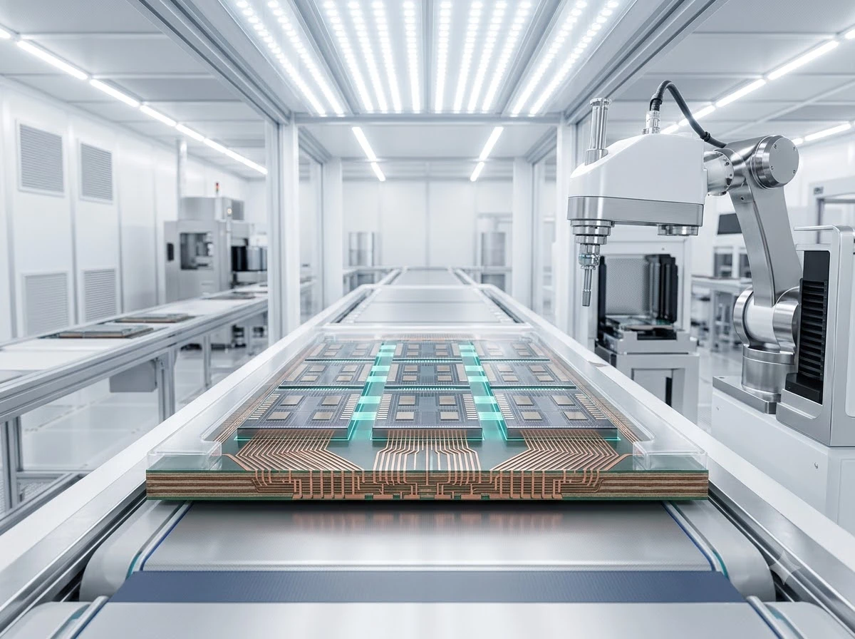
How Foveros Stacks Specialized Tiles
Foveros connects smaller chiplets on a silicon interposer. Chris Seibert, principal engineer at Fab 9, likens the interposer to a pizza crust. The chip-attach tool loads the crust wafer and the specialized “toppings,” then an oven bakes the stack. Epoxy underfills the gaps, and water-cooled blades dice the finished packages.
- Chip attach places chiplets from mixed designs or nodes onto the interposer wafer.
- Thermal bake and underfill lock the assembly for mechanical strength.
- Precision dicing yields individual multi-die packages ready for test.
The result lets power-hungry circuits sit on efficient nodes while the whole unit runs faster under heavy AI loads. Laptops thin out, edge devices shrink, and factory or desk systems pack more features into less space. Foveros Direct adds copper-to-copper hybrid bonding for even higher bandwidth and lower power in 3D stacks.
Each step in the flow is already production-proven. That maturity lowers the risk for external customers who want to move complex multi-tile designs into volume without reinventing the process line.
EMIB Bridges Cut Cost and Add Power Paths
EMIB embeds tiny high-speed silicon bridges only where chips need to talk inside the organic substrate. Other foundries often rely on a full expensive silicon interposer. Intel’s shortcut slashes material cost while still delivering the bandwidth AI demands.
EMIB mass production since 2017 covers both Intel and external silicon. For side-by-side data-center dies it creates direct bridges without a large wafer-scale layer. EMIB-T, rolling out in 2026, adds through-silicon vias in the bridge so power travels straight up instead of around the chips. That improves efficiency and routing for the newest high-bandwidth memory stacks.
Only Intel Foundry currently mixes chiplets from any source onto the industry’s largest substrates. That freedom supports the next wave of data-center AI engines.
Because the bridges occupy only the high-speed zones, the rest of the substrate can stay organic and lower cost. The savings compound as packages grow and the number of HBM stacks per module rises.
Specs That Push Past Reticle Walls
At ECTC 2026 Intel engineers showed concrete advances. First-layer interconnect bump pitch reaches 25 µm. Package form factors hit package form factors up to 120 x 120 mm. More than nine reticles of compute and memory silicon fit on one package. Signal integrity supports over 12 Gb/s for HBM4e and 64 Gb/s UCIe die-to-die links.
Key EMIB-T and Foveros metrics right now:
- Reticle scale: 8x industry standard today, targeting over 12x by 2028.
- Package size: up to 120 × 120 mm demonstrated.
- Content: more than 9× reticle silicon in a single package.
- Interfaces: >12 Gb/s HBM4e and 64 Gb/s UCIe.
One production example already in the field is the Intel Data Center GPU Max Series SoC: more than 100 billion transistors across 47 active tiles on five process nodes, all stitched with EMIB 3.5D plus Foveros.
| Technology | Interconnect style | Key advantage for AI | Production status |
|---|---|---|---|
| Intel EMIB / EMIB-T | Embedded silicon bridges + optional TSVs | Lower cost, power delivery direct to die, mix-and-match sources | Mass production since 2017; EMIB-T 2026 |
| Intel Foveros | 3D stacking on silicon interposer or hybrid bond | Vertical density, multi-node chiplets, smaller footprint | Mass production; Direct hybrid bond active |
| TSMC CoWoS | Full or local silicon interposer | Mature high-bandwidth volume for flagship GPUs | High-volume, capacity constrained |
EMIB avoids amortizing a full interposer across every design. That cost edge grows as packages get larger and HBM stacks multiply.
Where the Bottleneck Pressure Shows
TSMC still dominates leading-edge wafers and holds the bulk of advanced packaging volume. Yet CoWoS lead times and allocation fights have pushed hyperscalers and accelerator designers to dual-source. NVIDIA’s $5 billion investment in Intel, finalized late 2025, explicitly called out Foveros multi-technology packaging. Joint SoCs and CPUs for NVLink AI racks are slated for late 2027 or early 2028, with EMIB expected to take a meaningful share alongside TSMC.
Analysts note EMIB’s structure lets customers keep leading-edge logic at TSMC while shifting packaging steps to Intel. Google and others have explored similar paths. An Amkor partnership adds second-source assembly capacity for EMIB packages. Intel itself is adding packaging space for committed 2027 demand.
Skeptics on X still flag TSMC’s scale and yield maturity. One EDA product manager noted that “TSMC scale is on a different level” and wondered whether Intel can close the gap. Crowd chatter also watches thermal and defect rates on dense interconnects. Intel counters with AI-driven defect prediction already running on the packaging line and a foundry mindset that treats Intel silicon as just another customer.
Data Centers Feel the Density Gain First
Larger multi-die packages mean more compute and memory per rack unit. That raises power density even as EMIB-T and hybrid bonding improve efficiency per bit. Operators already building on-site power builds at AI data centers face the same pressure. Modular approaches such as modular factory-style AI pods become more attractive when the silicon itself packs tighter.
Heterogeneous integration also lets designers drop the right process node for each function-logic on the newest node, I/O or memory controllers on cheaper ones-without waiting for a monolithic shrink. The net effect is higher performance per watt and per square foot inside the hall, exactly what grid-constrained sites need.
- More silicon area per package raises rack-level compute density.
- Direct power vias and hybrid bonds offset some of the efficiency loss.
- Modular hall designs absorb the resulting thermal and power spikes more cleanly.
Roadmap Pieces Already Moving
- 2026: EMIB-T volume ramp with direct power vias for HBM4e-class memory.
- 2026-2027: Co-packaged optics edge connectors and glass-core substrate pilots for still-larger form factors and lower warpage.
- 2027-2028: Foveros-R RDL interposer production-ready; glass substrates move toward volume; NVIDIA co-packaged products target late 2027 or early 2028.
- By 2028: Package scaling past 12× reticle; hybrid bonding and through-glass vias mature for hyper-scale AI systems.
Glass substrates stay flat under heat where organic cores warp, enabling tighter alignment on the biggest packages. Detachable optical connectors aim to cut power and raise bandwidth for scale-up networks inside the rack. Hybrid-bonding research with partners keeps pushing die-to-wafer overlay and thermal limits.
Rio Rancho already offers silicon photonics manufacturing to external foundry customers and is positioned as an early volume site for glass. Sister packaging lines in Malaysia add geographic diversity. The combination gives customers a full U.S.-centric path from wafer to finished multi-die module when they want it.
Mix And Match Packaging Unlocks Design Freedom
The ability to place chiplets from any foundry on the same large substrate changes how teams allocate process nodes. Leading-edge logic can stay at TSMC while memory controllers, I/O dies, or custom accelerators arrive from other sources and still land inside one EMIB or Foveros package.
That separation of wafer and package supply chains is the practical answer to CoWoS allocation pressure. NVIDIA’s investment and the planned joint SoCs for NVLink racks show one path already under contract. Google and other hyperscalers have explored parallel routes for the same reason.
Amkor’s second-source role further spreads assembly risk. Customers can therefore treat packaging capacity as a flexible resource rather than a single-vendor bottleneck.
| Customer lever | How it works today | Benefit for AI systems |
|---|---|---|
| Logic at one foundry, package at Intel | EMIB or Foveros accepts external silicon | Bypasses full CoWoS queue while keeping advanced nodes |
| Multi-node tiles in one module | 47 tiles across five nodes already shipping | Right process for each function without monolithic wait |
| Second-source assembly | Amkor partnership for EMIB packages | Geographic and capacity redundancy |
Glass Substrates And Optics Stretch The Limits
Organic cores warp under the heat of large packages. Glass stays flatter, so alignment stays tighter as form factors push toward and beyond the 120 x 120 mm demonstrations already shown. That mechanical stability is why glass-core pilots appear on the 2026-2027 roadmap alongside co-packaged optics.
Detachable optical edge connectors target the scale-up networks inside the rack. Moving high-bandwidth links off copper reduces power draw and frees board real estate exactly when denser multi-die packages are raising both compute and thermal loads.
Rio Rancho’s existing silicon-photonics line for external customers positions the site as a natural early volume home for glass. The same U.S. campus can therefore carry a design from advanced packaging through photonic integration without crossing oceans.
Frequently Asked Questions
What is the reticle limit and why does it matter for AI chips?
The reticle limit is the maximum size a single photomask can expose in one step, roughly 800-850 mm² today. AI accelerators need far more silicon area for compute and HBM stacks, so packaging stitches multiple dies into one package that behaves like a giant monolithic chip while staying manufacturable.
How does EMIB differ from a full silicon interposer?
EMIB places small silicon bridges only in the substrate regions that need high-speed links. A full interposer is a large silicon slab under the entire package. The bridge approach uses less expensive silicon, shortens some signal paths, and simplifies supply chain and assembly while still hitting multi-terabit bandwidths.
When did Intel start high-volume EMIB production?
Intel has run EMIB in mass production since 2017 for both its own products and external silicon. The technology has already shipped in complex multi-tile data-center GPUs containing dozens of active dies across multiple process nodes.
What does EMIB-T add for high-bandwidth memory?
EMIB-T adds through-silicon vias inside the bridge so power can be delivered vertically straight to the dies rather than routed around them. That cuts IR drop and frees routing resources, which is critical when HBM stacks demand both high bandwidth and clean power delivery at the same time.
Can customers mix dies from different foundries on Intel packaging?
Yes. Intel Foundry’s process accepts chiplets fabricated on any process node or by any foundry and places them on the same large substrate using EMIB or Foveros. That mix-and-match flexibility is a core selling point for heterogeneous AI systems.
Intel’s packaging lines are no longer a supporting act. They are the route past the physical wall that once stopped AI chips from growing, and the open question is only how fast customers fill the new capacity.


South Korea Retail Investors Face Reckoning After KOSPI AI Rally Collapses

Surrey AI Maps Three Heart Attack Paths and Their Molecular Roots

Germany Locks Neutral Apple ATT Prompts Across Most of Europe

Apple’s 5% EU Fee Quietly Rewrites Alternative App Store Math

Apple’s EU Fee Truce Cuts Complexity but Leaves Rivals Fuming

Pixel 11 Pro Fold Trades Thinness for Durability and Seven-Year Stay

Mayo AI Flags HCM Obstruction From Everyday Ultrasound Videos

Indian Brands Quietly Scale Landmark Screens and Home Tech

Navin Vatsa Turns Grief Into a Lifetime of Quiet Seeing

Google Bets Pixel 11 Agentic AI Will Redefine Phones

Oracle Cuts 21,000 Jobs in a Year, Cites AI in 10-K Filing

Fable 5 and Mythos 5 Return as US Lifts Anthropic Export Controls

SpaceX’s Google Deal Turns a Rocket Company Into a Cloud Landlord

CD Projekt Red Co-CEO: Redemption Arc Isn’t Done, Witcher 4 in 2027

XPL Rallies 30% Ahead of Plasma One Card Tier Launch

Google Search Profiles Build a Follow Graph Inside Discover

DGO App Brings Rs 549 Mobile Pass for FIFA World Cup 2026 in Nepal

Moonshot AI Targets $30 Billion in China’s Fastest AI Funding Sprint

Oppo’s ColorOS 17 Eligibility List Leaves A-Series Buyers Behind

Microsoft Xbox Layoffs Start in July as Sharma Slams 3% Margin
-
 AI2 months ago
Oracle Cuts 21,000 Jobs in a Year, Cites AI in 10-K Filing
-
 AI2 months ago
Fable 5 and Mythos 5 Return as US Lifts Anthropic Export Controls
-
 AI3 months ago
SpaceX’s Google Deal Turns a Rocket Company Into a Cloud Landlord
-
 GAMING2 months ago
CD Projekt Red Co-CEO: Redemption Arc Isn’t Done, Witcher 4 in 2027
-
 CRYPTO3 months ago
XPL Rallies 30% Ahead of Plasma One Card Tier Launch
-
 NEWS3 months ago
Google Search Profiles Build a Follow Graph Inside Discover
-
 APPS3 months ago
DGO App Brings Rs 549 Mobile Pass for FIFA World Cup 2026 in Nepal
-
 AI3 months ago
Moonshot AI Targets $30 Billion in China’s Fastest AI Funding Sprint