
COMPUTERS
Nagoya’s Virtual Cathode Shapes Nanofilm Domes in 10 Seconds
Nagoya researchers drew a 1,200-nm dome on a graphene oxide nanofilm in 10 seconds with a computer-guided electron beam, below the 60-second light-based ceiling.

Nagoya University researchers used a computer-guided electron beam to form 1,200-nanometer dome bumps on a graphene oxide nanofilm within 10 seconds and to reshape those bumps on demand afterwards. The ‘virtual cathode’ technique, described in ACS Applied Materials & Interfaces on April 28, 2026, forms features ‘significantly faster than light-based methods,’ which the paper notes typically need 60 seconds or more for a single shape change, and does so without any fixed hardware electrode. Two open challenges still separate the lab from a living-cell interface: the film must operate in physiological electrolyte, and the team must learn to control where on the film the deformation actually starts.
From Sorting Sheets to Shaping Domes
In April 2025, first author Ken Sasaki and Professor Takayuki Hoshino at Nagoya published a paper in Colloids and Surfaces A showing that computer-drawn electric field patterns could sort graphene oxide sheets by size in solution. The setup replaced physical microfluidic devices with a programmable field that could appear, move, or vanish at a moment’s notice. A separate April 2025 announcement on size-sorting graphene oxide sheets captured the same result and listed Hoshino’s pitch for environmental and healthcare uses.
The 2026 paper shifts from sorting particles to bending a continuous film, a different mechanical problem. The lead author is the same Sasaki, the senior author the same Hoshino, with Associate Professor Hisataka Maruyama added to the author list at Nagoya University’s Graduate School of Engineering. Where the 2025 paper separated objects by their charge-to-mass ratio, the 2026 paper has to peel stacked layers off a substrate to produce a dome.
The 10-Second Dome
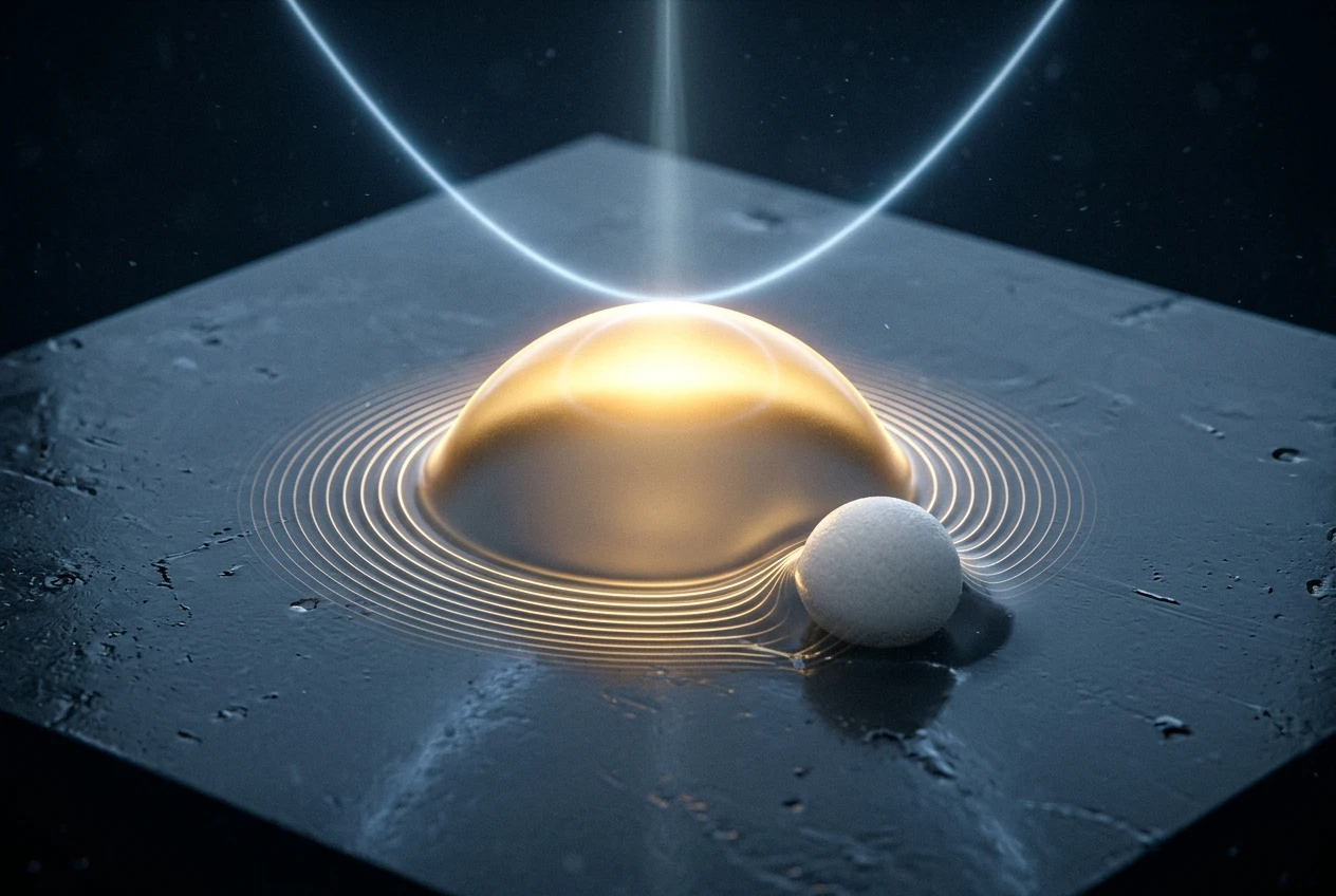
A dome-shaped bump roughly 1,200 nanometers high and 37 micrometers across formed on the film in that 10 seconds window.
Light-based reshaping methods typically need ‘60 seconds or more per shape change,’ the paper notes. Conventional electrical shaping, by contrast, ‘relies on fixed electrodes that restrict where reshaping can occur and limit the size of the change,’ the paper continues. The Nagoya technique is in the same speed league as the fastest electrical systems yet allows a computer to redraw the deformation zone on the fly. The headline figure is the dome’s height, which the authors describe as ‘significantly faster than light-based methods and matches the speed of the fastest electrical systems reported, but with a much larger height change.’ Both the position and the height of the bump are set by code rather than by lithography.
The deformation is reversible, the paper reports, which is what allows the technique to function as a ‘display’ rather than a stamping press. With the electron beam off, the dome flattens out and the film can be re-deformed at the same location. The team reshaped bumps into larger domes and into valley-like depressions by adjusting beam exposure and merging adjacent deformed regions. The film kept its structural integrity across the cycles the paper documents.
The paper’s funding statement lists two JSPS KAKENHI grants, 22K18775 and 23KJ0078, and a JKA Foundation grant, 2024M-563. Those grants paid for the same-spot reversibility data the supporting videos show. The paper closes by listing two open problems, both of which must be addressed before any cell-level work can run.
A Cathode With Nothing Inside It
The ‘virtual cathode’ name is the technical hook of the paper. In a conventional system, a shaped cathode is a piece of metal placed beneath the film, and the geometry of that metal sets the field that lifts the surface above. The Nagoya group inverted that chain: there is no metal cathode in the apparatus. Instead, an electron beam is scanned across a silicon nitride membrane along a computer-defined path, and the beam’s footprint on the membrane becomes, in effect, a moving cathode. Because the pattern is set by the scan path rather than by hardware, both its shape and its position can change instantly.
Sitting on top of the silicon nitride substrate is the second half of the innovation. The paper reports a multilayer film of pyrene-linked graphene oxide, about 45 nanometers thick and made of roughly 29 stacked layers anchored to the membrane. The film carries a negative surface charge in water. Exposure to the beam’s charged region drives electrostatic repulsion against the substrate below.
The repulsion peels the film into a dome. The mechanism, in the order the paper describes it, runs through five steps:
- The electron beam is scanned along a computer-defined path on the silicon nitride membrane.
- The beam’s footprint on the membrane generates a localized electric field, the ‘virtual cathode.’
- The negatively charged pyrene-linked graphene oxide film feels the field.
- Electrostatic repulsion against the substrate slides the stacked layers apart.
- The bottom layer peels away from the substrate, and the film bulges into a dome.
How the Team Sees a Feature Too Small to Touch
A 1,200-nanometer bump on a 37-micrometer footprint is invisible under a standard optical microscope. The Nagoya team observed the deformation in real time by leaning on graphene oxide’s own fluorescence, which normally does not exist for this material. Tightly stacked graphene oxide sheets quench each other’s fluorescence, the paper explains, so a flat, unstretched patch of the film appears dark. As the electron beam was applied, the film’s fluorescence switched on and intensified. That switch is the signal that the stack was separating, the paper says, because the layer spacing finally grew large enough to relieve the quenching.
As the film bulged, the changing thickness of the water layer between the dome and the substrate beneath produced interference patterns resembling the contour lines of a topographic map. Those patterns let the team measure height changes that fluorescence alone could not, in real time. Both signals together turned an invisible deformation into a tracked one. The two optical tricks explain how the team can report a 1,200-nanometer-tall bump on a 37-micrometer footprint without a direct image.
Pushing a Bead, Measuring Two Forces
The proof of concept for ‘shape can do work’ came from a 10-micrometer polystyrene bead. The team drove the bead across a water chamber by reshaping the dome underneath it, and the bead moved in the direction of the bulge. The force on the bead split into two measurable components, the paper reports.
| Rising under the beam | Subsiding after the beam turns off | |
|---|---|---|
| Speed range (paper) | 100 to 200 nanometers per second | 40 to 55 nanometers per second |
| Asymmetry label | Faster side | Slower side, in the ‘reversible but asymmetric’ behavior the paper names |
| Driver cited | Silicon nitride dielectric polarization builds up | Residual surface charge dissipates slowly |
Measured mechanical force from the moving surface: 0.05 piconewtons. Measured electrostatic repulsion from the charged film: 0.11 piconewtons. The paper calls the experiment suggestive, but not yet demonstrative, of the capability to move cells or to power microscopic robots. The asymmetry in the table above is what makes the bead push tunable: the 100 to 200 nanometer-per-second rise is the slow-control dial, and the 40 to 55 nanometer-per-second fall is the lag the system has to live with.
A key result from the paper: the same patch can be re-deformed after full recovery without visible damage across the cycles the paper documents. That repeatability matters less for moving a single bead than for any future setting where the surface is meant to deform many times in a row. The paper publishes four supporting videos, each showing a different reconfiguration: dome formation, dome merging, valley reshaping, and bead locomotion. In each clip, the film retains its structure.
Two Open Problems Before This Reaches a Cell
The two problems blocking a cell-ready system are spelled out at the end of the paper. The authors write that ‘precisely controlling where the film delaminates’ remains ‘an open challenge’ before living-cell work, as does ‘demonstrating stable operation in physiological electrolyte rather than pure water.’ Without those two, the system runs only in the distilled water the team’s experiments used.
We believe this technology will facilitate integration between nanomachines and computers. Nanoscale and microscale irregularities at interfaces are crucial for friction and adhesion between objects. This display technology can generate these irregularities on demand, which we hope will eventually enable control over the adhesion and assembly of microscopic cells and objects.
That statement is from senior author Takayuki Hoshino, included in the same Nagoya writeup that announced the result. The framing positions the bead push and the asymmetry data as one package: a programmable surface first, living-cell work still to come. The full April 2026 paper describing the new technique is open access.


South Korea Retail Investors Face Reckoning After KOSPI AI Rally Collapses

Surrey AI Maps Three Heart Attack Paths and Their Molecular Roots

Germany Locks Neutral Apple ATT Prompts Across Most of Europe

Apple’s 5% EU Fee Quietly Rewrites Alternative App Store Math

Apple’s EU Fee Truce Cuts Complexity but Leaves Rivals Fuming

Pixel 11 Pro Fold Trades Thinness for Durability and Seven-Year Stay

Mayo AI Flags HCM Obstruction From Everyday Ultrasound Videos

Indian Brands Quietly Scale Landmark Screens and Home Tech

Navin Vatsa Turns Grief Into a Lifetime of Quiet Seeing

Google Bets Pixel 11 Agentic AI Will Redefine Phones

Oracle Cuts 21,000 Jobs in a Year, Cites AI in 10-K Filing

Fable 5 and Mythos 5 Return as US Lifts Anthropic Export Controls

SpaceX’s Google Deal Turns a Rocket Company Into a Cloud Landlord

CD Projekt Red Co-CEO: Redemption Arc Isn’t Done, Witcher 4 in 2027

XPL Rallies 30% Ahead of Plasma One Card Tier Launch

Google Search Profiles Build a Follow Graph Inside Discover

DGO App Brings Rs 549 Mobile Pass for FIFA World Cup 2026 in Nepal

Moonshot AI Targets $30 Billion in China’s Fastest AI Funding Sprint

Oppo’s ColorOS 17 Eligibility List Leaves A-Series Buyers Behind

Microsoft Xbox Layoffs Start in July as Sharma Slams 3% Margin
-
 AI2 months ago
Oracle Cuts 21,000 Jobs in a Year, Cites AI in 10-K Filing
-
 AI2 months ago
Fable 5 and Mythos 5 Return as US Lifts Anthropic Export Controls
-
 AI3 months ago
SpaceX’s Google Deal Turns a Rocket Company Into a Cloud Landlord
-
 GAMING2 months ago
CD Projekt Red Co-CEO: Redemption Arc Isn’t Done, Witcher 4 in 2027
-
 CRYPTO3 months ago
XPL Rallies 30% Ahead of Plasma One Card Tier Launch
-
 NEWS3 months ago
Google Search Profiles Build a Follow Graph Inside Discover
-
 APPS3 months ago
DGO App Brings Rs 549 Mobile Pass for FIFA World Cup 2026 in Nepal
-
 AI3 months ago
Moonshot AI Targets $30 Billion in China’s Fastest AI Funding Sprint